I Can Hazwell?

Off-chip die is fairly large. Wonder what geometry it is manufactured with, I'd assume something coarser than 22nm, probably, seeing as DRAM is quite frugal with power, and older fabs are cheaper to run... Anyhow, damn nice piece of kit. I'm all hot and bothered now! :p

It definitely won't be 22nm, because DRAM does not need characteristics a logic focused process like Intel's process provides.

They probably got existing memory chip and integrated it with package.
 
Considering a 8Gb DDR-3 DRAM chip can be as small as roughly 10mm x 12mm (including package), I think it's possible that the off-die DRAM is 512MB ~ 1GB or larger. That'd be considerable if they are able to make the bus wide enough for sufficient bandwidth.
 
That'd mean 50+ percent of the die is GPU... Ugh! :D

So boring.... complete waste of precious space :cry:

Guys, why don't you tell them to stop screwing us and get their act as expected by normal sane people... :D

Some interesting comments from the Xtremes which I do like:

Seems like I will grow old with my 2600K. Does Intel really not want people with a Sandy or Ivy Bridge desktop chip to upgrade? Give us at least a 6 core as a minimum already!!! And I don't need silicon spend on an igpu.

this. Its been over 6 years since Q6600 was introduced. Its 2013 and still no mainstream 6 cores.. AMD's HSA seems more interesting than this :/

even haswell mobo's seem more of the same old no NGFF slot,No SATA Express, no integrated widi / miracast.. 99% of boards dont come with bluetooh 4.0 or wifi, no decent onboard sound.

and people wonder why PC growth is stagnant. :/
http://www.xtremesystems.org/forums...-Intel-haswell-i7-4770K-preview-article-TMSHW

Time for everyone to stop buying intel to get there attention. Tell everyone you know that builds, etc, then send intel a nice letter to go f*&k themselves. Maybe get there attention.

http://www.xtremesystems.org/forums/showthread.php?285764-Intel-Xeon-2013-2014-processors-detailed
 
Last edited by a moderator:
DRAM does not need characteristics a logic focused process like Intel's process provides.
Presumably intel is capable of tuning their process to manufacture different kinds of devices (they make flash for example in their own fabs, together with micron.) ...But presumably, it would be cheaper and more efficient to use spare fab capacity of a prior node, fabs that have already had all construction costs written off years ago most likely.

They probably got existing memory chip and integrated it with package.
Unpossible. That'd give the memory package far too little bandwidth. There's been talk that there's a 512-bit bus between the dies, indicating something custom-engineered. Also, seeing intel's big focus on power useage and saving these days, you'd think they'd want to cook up their own solution throughout, tailoring both devices on that substrate completely to their own requirements.
 
So boring.... complete waste of precious space :cry:

Guys, why don't you tell them to stop screwing us and get their act as expected by normal sane people... :D

Actually decent majority of the "normal people" do browsing and video playback as big part of their computing.

Catering to the minority would mean extremely small gain in revenue for lot more cost and work.
 
Presumably intel is capable of tuning their process to manufacture different kinds of devices (they make flash for example in their own fabs, together with micron.) ...But presumably, it would be cheaper and more efficient to use spare fab capacity of a prior node, fabs that have already had all construction costs written off years ago most likely.

Intel actually had separate flash fabs jointly operated with Micron. Micron has since bought out Intel's share: http://www.eetimes.com/electronics-news/4237169/Micron-buying-Intel-s-stake-in-two-IM-Flash-fabs

You can see at least one of these fabs also produced DRAM. AFAIK most DRAM manufacturers make NAND flash too so there's probably overlap in those processes but I don't think there is with the standard logic processes.

I'm not aware of Intel ever having eDRAM on a product made in one of their CPU fabs.. they could have had the capability but strikes me as a wasted investment for them since they're putting the DRAM off die. They very well could have had the die made by a collaborating party (Micron very well a possibility), of course that doesn't mean they're using off the shelf parts.

Unpossible. That'd give the memory package far too little bandwidth. There's been talk that there's a 512-bit bus between the dies, indicating something custom-engineered. Also, seeing intel's big focus on power useage and saving these days, you'd think they'd want to cook up their own solution throughout, tailoring both devices on that substrate completely to their own requirements.

There is the wide IO standard but that probably offers too little bandwidth per pin to be useful in this case. I don't really know if there's an intrinsic limitation in the technology that prevents companies like Samsung from making much higher clocked versions (that are not nearly as low power).
 
Actually decent majority of the "normal people" do browsing and video playback as big part of their computing

That is because they do nothing in order to promote heavy computing/ interesting games, etc, they do not innovate. They just left the desktops on inertia. Nothing new, nothing to get people's attention and money. One big nothing.

If you think that it's normal the most stupid tablet to have more extras than the premium motherboards, or the most stupid smartphone to have a retina display matching in resolution the big 20-30 inch monitors...

It depends how much the IGP's can be used for GPGPU. There's 400GFLOPs in that GT2 IGP which could do wonders for compute tasks.

Having said that another 4 Haswell cores would offer even more performance and be a lot more versatile so given the choice between 8 cores or 4 cores + GT2 at the same price point I'd certainly take the 8 cores any day.
 
Welcome to last decade...

360elite%20048.jpg
 
AFAIK most DRAM manufacturers make NAND flash too so there's probably overlap in those processes but I don't think there is with the standard logic processes.
The same machinery, chemicals and fundamental operations are used to manufacture all of these things. Intel could just as well set aside a production line to make these things inside one of their own facilities if they want to - which is likely exactly what they are doing. There's nothing stopping them from doing that.

I'm not aware of Intel ever having eDRAM on a product made in one of their CPU fabs..
Haswell DRAM die wouldn't require eDRAM tech. That's because it's not an eDRAM, it's off-chip, on-package. It would almost entirely 100% certainty be fabricated using standard DRAM techniques.
 
Personally I don't see what's so special about the "new package"...lol...from Intel.
Not sure what you're on tonight, reefer, LSD, PCP, nor do I particularly care. Nobody's really been commenting the package or shape of package of haswell - multi-chip modules aren't new. Intel once made a CPU called pentium pro - maybe you're too young to have heard of it. Wikipedia can tell you more. Btw, MCMs weren't new even then, they've existed in the big iron/supercomputer space well before they made it onto the consumer market.
 
In previous i-series chips, CPU cores were lined up in a row with L3 beneath them and the GPU tacked on to the side. Now I would assume that the GPU sits on the opposite side of the L3 compared to the cores, thus filling the chip out into a square-ish shape. That'd mean 50+ percent of the die is GPU... Ugh! :D
So? AMD has had more than 50% die size dedicated to GPU for Llano, Trinity, Richland, Zacate, Kabini, in fact all of their APUs including those for consoles of course (and in all but the first 3 cases FAR exceeding 50%).
 
AMDs APUs so far have had toy CPUs coupled to a fairly weak GPU. Haswell features the strongest general purpose CPUs in the market bar none, on the whole planet, coupled to what could be a medium-strength GPU, although maybe I'm over-estimating it, I don't really know. If I'm right(ish), that puts it rather into a class of its own methinks.

We'll likely know more after IDF, which is upcoming I recall reading somewhere (anandtech?) recently.
 
The same machinery, chemicals and fundamental operations are used to manufacture all of these things. Intel could just as well set aside a production line to make these things inside one of their own facilities if they want to - which is likely exactly what they are doing. There's nothing stopping them from doing that.

All I know is that there aren't a lot of companies that do both DRAM/NAND and things like processors, and the ones that do have separate foundries for it and use separately named processes, and not everyone offers eDRAM. I can't say if there's any real obstacle to putting DRAM on one of Intel's processes, outside of not necessarily having good libraries/designs for DRAM. What I can say is that foundries specializing in DRAM/NAND are currently using even smaller transistors than Intel's 22nm, since it's easier to shrink such a specialized and highly regular structure. So while I can't say for sure that Intel can't do it I know they can't do it as well as someone else can; whether or not this is worth the cost overhead I also couldn't say.

Haswell DRAM die wouldn't require eDRAM tech. That's because it's not an eDRAM, it's off-chip, on-package. It would almost entirely 100% certainty be fabricated using standard DRAM techniques.

It is eDRAM if it embeds the DRAM controller or anything else for that matter. If it doesn't then Intel is wasting some amount of die space on it for the GT3 parts that don't use it, but that could be the case (particularly if they're not making the die)
 
All I know is that there aren't a lot of companies that do both DRAM/NAND and things like processors, and the ones that do have separate foundries for it and use separately named processes, and not everyone offers eDRAM.

Note that eDRAM is not the same at all as traditional DRAM.

In modern high-density DRAM, the bit lines are on the substrate surface, the word lines are buried below the surface of the substrate, and the capacitors are formed by growing them on the top. This allows the capacitors to be very tall compared to the area they take, allowing them to have sufficient capacitance to retain data while taking minimal area. This allows for great bit density, using minimal process steps and conserving the need to use the most expensive equipment.

There's just one problem -- this process is completely incompatible with the kind of multi-layer, close to the transistor metal stacks that are needed for fast logic. You simply cannot form this kind of DRAM on the same chip you put a cpu on. Either your metal stack connects to the transistors through really tall vias (hello latency), or you'd basically have to eradicate either the metal stack or the capacitors to construct the other.

Winbond_Fig1_logo.jpg


eDRAM like the IBM variety is built by deep trench insertion, or boring the capacitors into the substrate, instead of building them on top of it. Then, you can build your tall metal stack on top of that and get logic and DRAM on the same chip. As an added benefit, eDRAM can be quite a bit faster because the transistors of the charge pumps can be closer to their metal stacks. As a negative, the process steps needed to bore very regular holes deep into the substrate and coat two sides of them with the plate material so that they can't touch each other are quite a bit more involved than what are used in normal DRAM, leading to much more expensive chips.

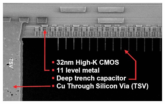
A good picture from IBM, showing logic, metal stack, DTI caps, and a TSV:

ibm-tsv-die-photo.gif


It is eDRAM if it embeds the DRAM controller or anything else for that matter.

This is a common misconception. Traditional DRAM and eDRAM differ by their structure, not by whether something is embedded or not. A full chip of eDRAM that embeds no logic is still eDRAM.
 
Would the on package RAM? DRAM? Be at all useful for general purpose CPU code? Most people running a high end CPU will probably have a discrete GPU anyway... Actually that is if the GT3e is available for desktop?
 
Would the on package RAM? DRAM? Be at all useful for general purpose CPU code? Most people running a high end CPU will probably have a discrete GPU anyway... Actually that is if the GT3e is available for desktop?

It would likely have latency not that much lower than the main ram, so it wouldn't do all that much as a cache. A clever programmer could in principle use it to add bandwidth by putting some often-used buffers there. I'd say that it likely would not be worth the effort and that no-one is going to do it.
 
Thanks for the information tunafish. Do you have any guess as to whether the separate die is eDRAM or not? It sounds like both traditional DRAM and eDRAM need special capability and are not necessarily something that a traditional logic fab can automatically provide..

This is a common misconception. Traditional DRAM and eDRAM differ by their structure, not by whether something is embedded or not. A full chip of eDRAM that embeds no logic is still eDRAM.

However, if it does embed other logic isn't it going to be eDRAM?
 
Back
Top