'Graphic North Bridge' PlayStation 4's Custom Chip?

onQ

Veteran
Some times the answer can be right under our nose & we never see it.


Remember the sweetvar26 post about the PS4 chip? http://forum.beyond3d.com/images/icons/postnv.gif


PS4:

New Starsha GNB 28nm TSMC
Milos
Southern Islands

DX11
SM 5.0
Open CL 1.0
Quad Pixel pipes 4
SIMD’s 5
Texture Units 5TCP/2TCC
Render back ends 2
Scalar ALU’s 320

EDIT: Some of those were crossed, may be they were updated/changed at a later date, I have no idea.
Quote:
Couple of more updates

Graphic North Bridge(GNB) Highlights
Fusion 1.9 support
DCE 7.0
UVD 4.0
VCE
IOMMU
ACP
5x8 GPP PCIE cores
SCLK 800MHz/LCLK 800MHz


Pretty weak compared to the PS4 GPU huh?

wait what the hell is a 'Graphic North Bridge'?

google & what do you find?

http://www.indeed.com/r/Rami-Dornala/e0704aad508659b2

Rami Dornala
Waltham, MA
Work Experience
Graphic processor
AMD - Waltham, MA
September 2011 to Present
Project:1 GNB core SOC
Duration: Sept 2011 , till date
Location: AMD
Description:
GNB core is based on the AMD fusion core technology, The GNB is a fusion of Graphic processor, power optimizer, audio processor, south bridge and north bridge which share a common interface with system memory.

Role: Tech Lead, Was responsible for Delivery of verification for Tapeout
Contribution:
1. Responsible for Functional verification of GNB.
2. Integrated ACP IP into the GNB environment
3. Integrated ISP IP into the GNB environment.
4. Aware of BIA, IFRIT flows.
5. Responsible for SAMARA and PENNAR integration.
6. Involved in kabini coverage closure, involved in LSC for kabini
7. Involved in fc mpu integration.
8. ONION and GARLIC bus OVC understanding and GNB environment set up for samara database.
9. Involved in LSA for Samara and Pennar GNB's
10. Involved in setting up of Pennar database with GF libraries
9.Involved with migration of Pennar database from TSMC to GF libraries.

Team Size: 12
Technology used:
Verification environment is a hybrid mixture of System-C, SystemVerilog and C++ language.GNB is targeted for 20nm technological library with GF foundaries.
Project:2 G4Main SOC


oh so it's a Graphic North Bridge yeah that make's sense! wait no it doesn't this is just as crazy as Mark Cerny saying that the PS4 custom chip is a south bridge.


these people are crazy


wait what? ONION and GARLIC where have I seen that before?


lvp2.jpg


& there you have it.

secondary-ps4-chip-e1361421157584.png
 
Last edited by a moderator:
What do you think this proves? AMD has a name for the "GPU+memory interface+highspeed interconnect" part of the APU. So? There's no new information here.
 
I wonder if Durango has some form of this as well, as it seems to be a standard part of their whole Fusion APU architecture.

Back in the early 14+4 days I was pretty sure that '320 Scalar ALU' had some kind of relation to that split or enhancement of 4 CU. Hope there's more to reveal at E3.
 
Some times the answer can be right under our nose & we never see it.
Remember the sweetvar26 post about the PS4 chip? http://forum.beyond3d.com/images/icons/postnv.gif
Pretty weak compared to the PS4 GPU huh?
wait what the hell is a 'Graphic North Bridge'?
google & what do you find?
http://www.indeed.com/r/Rami-Dornala/e0704aad508659b2
oh so it's a Graphic North Bridge yeah that make's sense! wait no it doesn't this is just as crazy as Mark Cerny saying that the PS4 custom chip is a south bridge.
these people are crazy
wait what? ONION and GARLIC where have I seen that before?
& there you have it.

I'm sorry, can you put all that into a sequence of related complete sentences with that express a concrete theme or set of themes, while providing some kind of analysis as to why each piece of data fits into the whole?

If you're trying to tie that post to the idea of the custom southbridge chip for the PS4, your links only make sense if you only use every other word and reverse the meaning of the remainder.


Yes this is the Custom Chip & it's also what Eurogamer was talking about.

Additional hardware: GPU-like Compute module, some resources reserved by the OS

However, there's a fair amount of "secret sauce" in Orbis and we can disclose details on one of the more interesting additions. Paired up with the eight AMD cores, we find a bespoke GPU-like "Compute" module, designed to ease the burden on certain operations - physics calculations are a good example of traditional CPU work that are often hived off to GPU cores. We're assured that this is bespoke hardware that is not a part of the main graphics pipeline but we remain rather mystified by its standalone inclusion, bearing in mind Compute functions could be run off the main graphics cores and that devs could have the option to utilise that power for additional graphical grunt, if they so chose.
 
Maybe I'm being dense, but I don't see what lends itself to that conclusion.

The data points provided spell out devices whose feature sets, technologies, and functions have zero described overlap.
 
Yes this is the Custom Chip & it's also what Eurogamer was talking about.

It isn't. A GNB is part of any APU, with as many or as few shaders as AMD wants. It has nothing to do with the south bridge and it has nothing to do with any secret "bespoke" compute module, which was probably just a misunderstanding of the beefed up ACEs either on Eurogamer's part, or heir source's.
 
doesn't the description say the GNB is both a north and south bridge???

Yes.

"GNB core is based on the AMD fusion core technology, The GNB is a fusion of Graphic processor, power optimizer, audio processor, south bridge and north bridge which share a common interface with system memory."


"Realizing Energy Efficiency and Smoothness using a Second Custom Chip with Embedded CPU
Cerny: The second custom chip is essentially the Southbridge. However, this also has an embedded CPU. This will always be powered, and even when the PS4 is powered off, it is monitoring all IO systems. The embedded CPU and Southbridge manages download processes and all HDD access. Of course, even with the power off."
 
doesn't the description say the GNB is both a north and south bridge???

No, OnQ found a guy who worked on a version of GNB who describes that version as integrating south bridge functions, but that does not mean that is true of every GNB, nor rule out the implementation of an additional off chip south bridge.
 
Hey guys, I found that Onion and Garlic were used in Llano and now they're showing up in PS4 documentation.. who would have thought PS4 is using Llano?
 
Yes this is the Custom Chip & it's also what Eurogamer was talking about.
No. They said with the 8 CPU cores there's a GPU compute unit. Well guess what the 18 CUs are used for? ;) That's clearly a muddling of the information, I guess based on AMD working to make compute more seamless across processing cores so the same high-level code works on CPUs and CUs. If what you say is true, Sony revealed Ps4 but withheld the fact they have additional compute on top of the GPU.
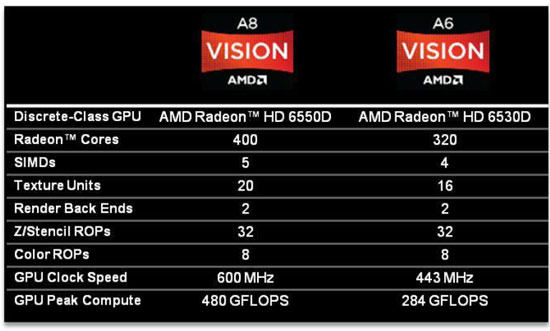
No.

"GNB core is based on the AMD fusion core technology, The GNB is a fusion of Graphic processor, power optimizer, audio processor, south bridge and north bridgewhich share a common interface with system memory."
The Fusion architecture incorporates NB. GNB is nothing more than Liverpool as we've already been told it. a CPU+GPU+north bridge glue with extra processing like audio and video. We may have an extra audio DSP in there or the like. This is standard for Fusion.

"Realizing Energy Efficiency and Smoothness using a Second Custom Chip with Embedded CPU
Cerny: The second custom chip is essentially the Southbridge. However, this also has an embedded CPU. This will always be powered, and even when the PS4 is powered off, it is monitoring all IO systems. The embedded CPU and Southbridge manages download processes and all HDD access. Of course, even with the power off."
This is the ARM-incorporating Southbridge needed for low-power mode. What has that got to do with a high-power APU Northbridge?

In summary, Sony revealed their hardware and didn't secretly hide any performance power (we've another 400 GFlops of compute on our graphics northbridge that we don't want to tell anyone about. Tee hee). There's an AMD Fusion APU called Liverpool that incorporates northbridge and some ancillary processing. There's the southbridge with low power CPU (ARM) to comply with the EU's power requirements and that'll manage background functions like downloading in standby. That's it. There's nothing more to see except mirages.

And please don't bold and red. Making something bright red doesn't communicate it any more effectively to our dim-witted brains. If you're making a point and we're not agreeing, using larger and more colourful fonts isn't going to sway us any more. Jeff Rigby didn't get very far with all his colourful and oversized texts...
 
The Fusion architecture incorporates NB. GNB is nothing more than Liverpool as we've already been told it. a CPU+GPU+north bridge glue with extra processing like audio and video. We may have an extra audio DSP in there or the like. This is standard for Fusion.

This is the ARM-incorporating Southbridge needed for low-power mode. What has that got to do with a high-power APU Northbridge?

In summary, Sony revealed their hardware and didn't secretly hide any performance power (we've another 400 GFlops of compute on our graphics northbridge that we don't want to tell anyone about. Tee hee). There's an AMD Fusion APU called Liverpool that incorporates northbridge and some ancillary processing. There's the southbridge with low power CPU (ARM) to comply with the EU's power requirements and that'll manage background functions like downloading in standby. That's it. There's nothing more to see except mirages.

But if the Leak was real no way that it could have been the whole PS4 APU because it was too weak.


SIMD’s 5
Texture Units 5TCP/2TCC
Render back ends 2
Scalar ALU’s 320


that's between a A6 & A8 APU

amd-vision.jpg
 
But if the Leak was real

But ... But ... But ... But nothing. Give up the delusions of magical secret units offering power of the universe.
 
But ... But ... But ... But nothing. Give up the delusions of magical secret units offering power of the universe.

Huh? I'm not saying that it's a magical secret units.


I'm saying that it's a part of the PS4 that we already heard about.


Additional hardware: GPU-like Compute module, some resources reserved by the OS

However, there's a fair amount of "secret sauce" in Orbis and we can disclose details on one of the more interesting additions. Paired up with the eight AMD cores, we find a bespoke GPU-like "Compute" module, designed to ease the burden on certain operations - physics calculations are a good example of traditional CPU work that are often hived off to GPU cores. We're assured that this is bespoke hardware that is not a part of the main graphics pipeline but we remain rather mystified by its standalone inclusion, bearing in mind Compute functions could be run off the main graphics cores and that devs could have the option to utilise that power for additional graphical grunt, if they so chose.
 
Who is sweetvar ?

The 14+4 CU rumor corresponds to the GPU's unified 18 CUs.

DF's "GPU-like Compute module" note is intriguing. However, Eurogamer also commented that the custom secondary chip is ARM based. I suggest we wait for more leaks before speculating about this Starsha spec.

The other APU spec leaks were corroborated by multiple sources. The only source for StarSha is sweetvar. For all we know, if such a thing exists, it could be for another unrelated project in Sony.
 
I thought the whole "14+4" idea was debunked and discarded from the general consensus of what is in the PS4 hardware. Are there still some people holding onto the notion that there's a CU block separate from the GPU part? Maybe that was an earlier iteration of the hardware before it was finalized. Either way it is better to have 18 CU's that can work on graphics and compute.
 
Back
Top