Install the app
How to install the app on iOS
Follow along with the video below to see how to install our site as a web app on your home screen.
Note: This feature may not be available in some browsers.
You are using an out of date browser. It may not display this or other websites correctly.
You should upgrade or use an alternative browser.
You should upgrade or use an alternative browser.
G71/G73: Summary & Pre-Launch Speculation Frenzy
- Thread starter Arun
- Start date
NocturnDragon
Regular
dizietsma said:Conroe and quad Sli come H2 looks like it might be nice .. plus whatever large LCD monitor is the best then.
AEG .. PM me at will, no serious offers refused !LOL
a large LCD monitor? naaa 3 LCD monitors! Let's the surround gaming begin!!!!
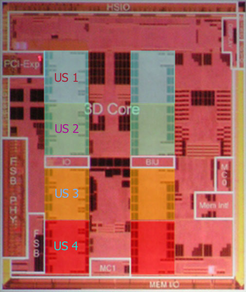
Jawed said:I have coloured in what I think are the four shader arrays of this chip - each array appears to be split in two, either side of what I guess is scheduling/queueing/back-end type functionality.
I see it differently. I see multiples of 6x everywhere.
Take the left strip of what you have marked as US1-4. The left side of it has 12 small rams. The right side also.
The right strip has also 12 rams per US on the left side. Only the right side of the right strip has 4 RAMs. You say that it has a 16-pipe texture unit, so this could explain the multiple of 4.
A factor of 6 is quite unusual. Connect this with the fact that there are 48 pipeline and it becomes fairly obvious to me.
Jawed said:The chip is supposed to be around 232M transistors, and each shader array appears to consume about 8% of the die.
Finally, this GPU offers only 48 active pipelines - yet the design appears to consist of 4 arrays, each of 16. i.e. though architected for 64 pipelines, 16 appear to be dropped for redundancy.
In summary, only 8% of this die is consumed by shader array redundancy - if my theory is correct.
It think it's highly unlikely. Going forward, I'm sure Microsoft plans to shrink this chip to smaller technologies. A 200mm2 die in 90nm becomes 100mm2 in 65nm, resulting in much better yields. Go to 45nm and you're at 50mm2, at which point the redundancy really becomes pointless.
Jawed said:As a matter of interest, at a guess, R580's fragment shader pipelines (if there are really 64, with 16 dropped for redundancy) would consume about 33% of the entire die: 128M transistors out of 384M.
Jawed
Even more unlikely: the math simply doesn't add up. Redundancy pays off much more when you can selectively enable or disable small portions of a die, like a row or a column of a RAM. (Or, like the PS3 cell with 1 redudant SPE out of 8.) A 33% redundancy won't help if you have 2 defects in 2 different pipelines.
Let's assume for a momenet that there were 64 shaders: it means there must be a number of dies coming out of production with all pipes operational. ATI would be crazy not to market those as some kind of ultra high performance $800 card that beats the competitor silly.
That's also why I don't think that the G70 has a dark quad, as suggested by geo and others: the majority of the dies go to the relatively high-volume 7800GT and 7800GS products which have 1 defective quad. Only the few parts with all quads working go to the GTX, which you price high enough to prevent mass demand. Makes perfect sense: you never waste silicon and get highest return per wafer.
There are no "dark quads" on G70.
http://www.theinquirer.net/?article=30130
Geforce 7900 GTX works at 650MHz core and 1600MHz memory. The chip is developed on 90 nanometre marchitecture and has 278 million transistors.
http://www.theinquirer.net/?article=30130
serenity said:Reports flowing in from Cebit suggesting no new features ..
Hope dies hard.
But there's always the wake to look forward to! 278 million transistors..INQ has been saying it's RSX all along. Granted with new memory interface.
Not sure how this jives with Sony's 300 million plus transistors E3 slide.
Also puts it that much closer to Xenos size.
Also 278 vs 384. And the 278 will probably be highly competitive. Wow.
Not sure how this jives with Sony's 300 million plus transistors E3 slide.
Also puts it that much closer to Xenos size.
Also 278 vs 384. And the 278 will probably be highly competitive. Wow.
Ailuros said:
We agree.
Not clear though how you can prove this with a link about G71
Pretty much. I want to link the G71 review in my sig, its getting itchy over there.geo said:Hope dies hard.
By the way, 7900 GT Preview
Xbot360 said:Hardocp forums say NDA expires at 3 AM Eastern.
Awesome. 2 AM Central. I'm normally up all night anyway.
Hmm. Timed to coincide with the show-opening in Hannover? Or were they speculating? The standard of late seems to be 9am Eastern. Well, I'm going to bed. If some show up, someone please start a new thread in Graphics Cards for them, "GF7900 Reviews" and "GF7600 Reviews" or something of the like. . .
Hmm. Timed to coincide with the show-opening in Hannover? Or were they speculating? The standard of late seems to be 9am Eastern.
I dunno they said 12PST.
I think this is too good to be true though. But I'm hoping. Yeah it's usually 9 AM.
serenity said:Pretty much. I want to link the G71 review in my sig, its getting itchy over there.
By the way, 7900 GT Preview
"The eVGA 7900GT retail unit used eVGA's traditional package design as well as assortment of accessories. On the front of the packaging is an image of this PCI Express graphics card as well as listing some of its features -- 550/1580MHz, GDDR3, 256MB,"
550/1580 is not too shabby indeed. Should be able to get another 40-50Mhz ontop as well I would guess. Is this going to be a real bargain do you think ?
Pictures of boxes at rage3d
http://www.rage3d.com/board/showthread.php?p=1334215314#post1334215314
So Clubic confirms what's already been said. G71's lost some transistors (and presumably power draw) while gaining clocks and twice the per-clock blending capability.
Their #s are interesting. On the one hand, (the 7900's) generally (far) superior "plain" framerates have in the past meant better performance in future games. OTOH, who's to say (ATM, anyway) if future games better exploit (the X1900's) extra shader ALUs and so such an architecture would mature more gracefully?
With AA+AF, it doesn't look like ATI's hurting (just don't look too hard at power and heat). In fact, comparing a 650/1600 7900GTX to a 650/1550 X1900XTX is the closest we'll get to a clock-for-clock comparison in a while (without fretting about RAM timings). Good stuff.
The BF2 #s are pretty funny. See NV embarass ATI without AA or AF. Turn on AA and AF and see ATI embarass NV, thanks to NV dropping 50% but ATI a mere 10% (from the X1800XL to the X1900XTX). I can't tell if this means the demo is a bit of useless, if ATI don't bother going the whole nine yards without AA+AF, or if R5x0 just rocks AA+AF efficiency (given the same bandwidth).
Oh, does G71 have a higher-clocked vertex domain, or is it 650 through and through?
Jawed
Legend
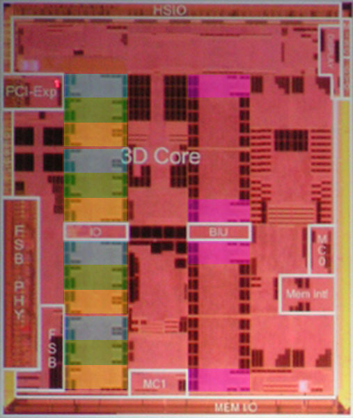
I have produced an alternative picture to better-illustrate the layout as I understand it:

In Cell each SPE is 21M transistors, 14M RAM and 7M of logic. Each SPE is ~6% of the die (taken from a die photo I have here).
In Xenos each shader array is ~8% of the die.
In R580, if my estimates are reasonable, 8.3% of the die is given up in redundancy - 2M transistors per pipeline with four pipelines being redundant per shader unit, equals a total of 32M transistors (out of 384M). The 2M figure actually needs revising down - because it's based on 64M extra transistors in R580 over R520, corresponding to an extra 32 pipelines, which doesn't include the redundant 16 pipelines that I'm hypothesizing, nor other tweaks such as Fetch-4... But, anyway, 8% seems like a reasonable starting point, even if it's high.
I think it's pretty interesting that all three come out in the range of 6-8%
Will Sony revisit 1-SPE redundancy in PS3's version of Cell, in the 65/45nm future? Whilst Cell is on 90nm, what percentage of all Cells produced are going into PS3? 99%?...
I'm not saying every R580 on a wafer will work, simply that it's possible to cut the yield cake in different ways to get ~ the same margins.
Jawed
As you can see from the picture above, the die looks like it's easily split into four groups of four, each block being a "quad-pipeline".silent_guy said:I see it differently. I see multiples of 6x everywhere.
Take the left strip of what you have marked as US1-4. The left side of it has 12 small rams. The right side also.
The right strip has also 12 rams per US on the left side. Only the right side of the right strip has 4 RAMs. You say that it has a 16-pipe texture unit, so this could explain the multiple of 4.
A factor of 6 is quite unusual. Connect this with the fact that there are 48 pipeline and it becomes fairly obvious to me.
I doubt M$ can do those shrinks, so ATI will be contracted to perform them. There's no reason why redundancy couldn't be revisited at each node. Is there?It think it's highly unlikely. Going forward, I'm sure Microsoft plans to shrink this chip to smaller technologies. A 200mm2 die in 90nm becomes 100mm2 in 65nm, resulting in much better yields. Go to 45nm and you're at 50mm2, at which point the redundancy really becomes pointless.
Cell is partly the basis for my view of R580 redundancy - an entirely dark SPE is no different, conceptually, from an entirely dark shader array in XenosEven more unlikely: the math simply doesn't add up. Redundancy pays off much more when you can selectively enable or disable small portions of a die, like a row or a column of a RAM. (Or, like the PS3 cell with 1 redudant SPE out of 8.) A 33% redundancy won't help if you have 2 defects in 2 different pipelines.
In Cell each SPE is 21M transistors, 14M RAM and 7M of logic. Each SPE is ~6% of the die (taken from a die photo I have here).
In Xenos each shader array is ~8% of the die.
In R580, if my estimates are reasonable, 8.3% of the die is given up in redundancy - 2M transistors per pipeline with four pipelines being redundant per shader unit, equals a total of 32M transistors (out of 384M). The 2M figure actually needs revising down - because it's based on 64M extra transistors in R580 over R520, corresponding to an extra 32 pipelines, which doesn't include the redundant 16 pipelines that I'm hypothesizing, nor other tweaks such as Fetch-4... But, anyway, 8% seems like a reasonable starting point, even if it's high.
I think it's pretty interesting that all three come out in the range of 6-8%
Will Sony revisit 1-SPE redundancy in PS3's version of Cell, in the 65/45nm future? Whilst Cell is on 90nm, what percentage of all Cells produced are going into PS3? 99%?...
If the despatcher is architected to issue 4-phase x 12 fragment threads (48 fragments per thread), it might not have the capability to issue 4x16 threads (64 fragments per thread).Let's assume for a momenet that there were 64 shaders: it means there must be a number of dies coming out of production with all pipes operational. ATI would be crazy not to market those as some kind of ultra high performance $800 card that beats the competitor silly.
ATI used to do this with X800. All I'm suggesting is that ATI's moved on to a yield model that tries to ensure that every die works, with redundancy hidden inside the die due to the massively parallel nature of the architecture - rather than relying upon binned (or trashed) dies.That's also why I don't think that the G70 has a dark quad, as suggested by geo and others: the majority of the dies go to the relatively high-volume 7800GT and 7800GS products which have 1 defective quad. Only the few parts with all quads working go to the GTX, which you price high enough to prevent mass demand. Makes perfect sense: you never waste silicon and get highest return per wafer.
I'm not saying every R580 on a wafer will work, simply that it's possible to cut the yield cake in different ways to get ~ the same margins.
Jawed
Last edited by a moderator:
DegustatoR
Legend
700 for geometry.Pete said:Oh, does G71 have a higher-clocked vertex domain, or is it 650 through and through?
Similar threads
- Replies
- 460
- Views
- 75K