
Bondrewd
Veteran
If it was a mesh, yes.MI300 has 4.8 TB/s bidirectional bisection bandwidth, that's less than half B100
again, people will bench the MALL soon™.
If it was a mesh, yes.MI300 has 4.8 TB/s bidirectional bisection bandwidth, that's less than half B100
So you're saying AMD are just lying in their white paper?If it was a mesh, yes.
again, people will bench the MALL soon™.
Doesn't say anything about AID topology, no.So you're saying AMD are just lying in their white paper?
Any IHV having a bandwidth advantage would definitely be in broadcasting mode.MI300 has 4.8 TB/s bidirectional bisection bandwidth, that's less than half B100
Sorry, not their white paper, their slide deckDoesn't say anything about AID topology, no.
Yeah, this only applies if this was an Intel-style mesh.Sorry, not their white paper, their slide deck
Specifically this one: https://regmedia.co.uk/2023/12/06/amd_mi300_wire_rates.jpg
They do link compression and a lot of routing hacks.In that case effective bandwidth is surely much less than the ~10.8TB/s aggregate of all the links.
Yes. A single XCD can access it's own HBM at 1.33 TB/s and the neighbor's at 1.2-1.33 TB/s with latency penalty.Is that picture accurate? Do data transfers from top left to bottom right have to make an additional hop through one of the adjacent dies? In that case effective bandwidth is surely much less than the ~10.8TB/s aggregate of all the links.

Naturally, addressing the remote stacks will incur latency penalties. Memory transactions incur more latency the further they travel. AMD noted that HBM connected directly to the IOD and XCD is a zero-hop transaction while accessing a different memory stack on the IOD is a two-hop jump. Finally, accessing a memory stack on an adjacent IOD is a three-hop jump. The penalty for a two-hop jump is roughly a 30% increase in latency, while a three-hop jump adds 60% more latency. -Tom's Hardware-

 www.nextplatform.com
What this means is a rack with 72 Blackwell GPUs is the new unit of performance that is replacing an eight-CPU node using H100 or H200 or even B100 or B200 GPUs. Not that you will not be able to buy those DGX servers and clones of them from OEMs and ODMs that in turn buy HGX GPU complexes from Nvidia.
...
Here are the feeds and speeds on the HGX B100 and HGX B200 and their B100 and B200 GPUs, which are included in the Nvidia Blackwell Architecture Technical Brief:
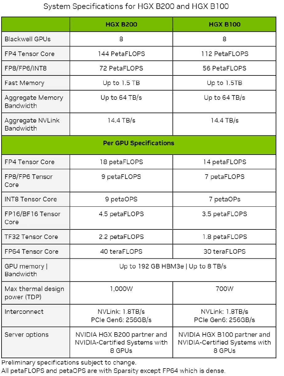
All of the throughput shown at the various precisions and data formats are expressed with sparsity on except the FP64 throughput, which is shown with sparsity turned off.
What immediately jumps out to us is that all data is shown running on tensor cores, not CUDA cores. That doesn’t mean there are no CUDA cores in the Blackwell architecture, but it is odd that they are not shown if they are there – and interesting if there are no CUDA cores. (Our hunch is that there are none, and we are sitting in on an architectural briefing later this evening to find out.)
...
The B100 used in the HGX B100 GPU complexes has the same thermals as the H100 used in the GHX H100 GPU complexes, so any system that was designed for these Hopper H100 SXM5 GPUs can used the Blackwell B100 SXM6 module, which delivers 14 petaflops at FP4 and 7 petaflops at FP8. At FP8 precision, that is 1.8X more throughput per Blackwell die compared to the Hopper die, and there are two of them, which yields a 3.6X increase in FP8 performance. This strongly suggests to us that there are around 2X more tensor cores on the Blackwell die than on the Hopper die.
...
That 2:1 ratio of GPUs to CPUs shows that having Grace be so powerful was not necessary for AI hosts, and even the adjunct LPDDR5 memory was not needed as much as it is for the embeddings that are used for recommendation engines. Grace only has a 600 GB/sec NVLink 4.0 port coming out of it, and this is split into two, using 300 GB/sec to chat to each Blackwell B200 GPU. That’s a lot more than PCI-Express can do, and in fact, it will be early next year before we have 256 GB/sec PCI-Express 6.0 x16 slots. The 1.8 TB/sec bandwidth that Nvidia will deliver this year with NVLink 5.0 ports won be available until around 2032 with PCI-Express 9.0 x16 slots delivering 2 TB/sec at that time.
Going by AMD's slide only three of the IODs can access the HBM from two others with full speed. 1/4 of MI300X is like the Grace-Hopper superchip - a memory expansion. That is totally different to Blackwell. One chip has access to all HBM memory at full speed and has twice as much L2 cache than Hopper.Yes. A single XCD can access it's own HBM at 1.33 TB/s and the neighbor's at 1.2-1.33 TB/s with latency penalty.
View attachment 11030
Edit: Oh wait..
View attachment 11032
One chip has access to all HBM memory at full speed and has twice as much L2 cache than Hopper.
Don’t think that’s fair to MI300X, any real workload will be randomly distributed across the HBM stacks, and there’s more than enough bandwidth to hit 100% HBM utilisation. The theoretical bottleneck is for the L3 where you can’t use 100% of the L3 bandwidth for similar cases, but it’s still fairly high. Kinda suspect H100 “near L2 only” bandwidth is similarly higher than what can be used in practice fwiw but haven’t tested that properly yet.Going by AMD's slide only three of the IODs can access the HBM from two others with full speed. 1/4 of MI300X is like the Grace-Hopper superchip - a memory expansion. That is totally different to Blackwell. One chip has access to all HBM memory at full speed and has twice as much L2 cache than Hopper.
GH200 shares the same 'issue' aka the reason it pretty much doesn't exist outside of select* HPC deployments.FWIW, I learned that GB200 NVL72 is 1 address space per “1 Grace, 2 Blackwells” (384GiB HBM3E, 480GiB LPDDR5X).
Little sleep deprived so I could be wrong...NVIDIA is being intentionally very silent about anything Blackwell at GTC in general though, I literally can’t even remember seeing it mentioned on any of the slides of any of the CUDA presentations except for fp4 support without any details (I missed Bill Dally’s presentation and the talk about Tensor Engine API so not sure if they said anything about it there).
Do you mean on the CPU/Grace side? I don’t know much about that tbh, but on the GPU side it’s not like anyone else has a single address space and the bandwidth to make it very useful AFAIK.GH200 shares the same 'issue' aka the reason it pretty much doesn't exist outside of select* HPC deployments.
NVIDIA is being intentionally very silent about anything Blackwell at GTC in general though, I literally can’t even remember seeing it mentioned on any of the slides of any of the CUDA presentations except for fp4 support without any details (I missed Bill Dally’s presentation and the talk about Tensor Engine API so not sure if they said anything about it there).