28nm : Why Nvidia overclocks better??

gongo

Regular
Just a question of interest...on average Nvidia 28nm lineup seems to have 25-35% (40% on lottery wins) more overclocking headroom from their stock speeds...even the modest 750Ti, just on PCIE power, can hit 1.25-1.3Ghz on core! And of course their 'big' cores can hit the same range, on stock air cooler! Impressive!

AMD meanwhile tops out at around 1.15Ghz on their cores, regardless of their models, that is without going into insane voltage territories. ..

Is it because Nvidia uses less GPU cores (SM) but run those at higher clocks?

Will a 1.15Ghz FuryX stand tall against a 1.3Ghz 980Ti???
 
It depends on the target clock speed the silicon was designed for. If GCN was designed for, say, 900MHz and Maxwell for 1000MHz, then it's only normal that the latter will go to higher clocks in general.

That, and architectural reasons: it could be that the critical path in one is in a place with lots of levels of logic while it's just routing delay in the other. The former will overclock better than the latter.
 
Nvidia OC also works differently than AMD OC because nvidia's boost clocks are already above the normal frequency which AMD has a max target for frequency. Overall, the performance gains from OCing cards from both companies are about the same. Both has about a 20% OC headroom for performance.

People have gotten 1300mhz out of AMD cards too and they probably happen as often as the1500mhz nvidia overclocks.
 
Nvidia cards would actually OC much higher than they do right now if they allowed voltage control.

Part of the reason why I liked the original titan so much. Mine could bench at 1500MHz (50%+ OC) and run games at 1400MHz (40%+ OC) because it had proper voltage control.
 
Overclock is a rather subjective term. Overclock over what? nVidia's target clocks? Factory-overclocked clocks?
A more interesting question would be why nVidia's cards are clocking so much higher than AMD's at equivalent die areas, despite the lower power consumption and the fact that they're using the same 28nm process.

For example, GM204 is 400mm^2 large, clocks at 1125-1215MHz and consumes up to 165W.
Hawaii XT is 440mm^2 large, clocks at 1000MHz and consumes up to 290W.

One thing that comes to mind is that Hawaii has a higher transistor density. They have about 20% more transistors for a 10% larger chip. Denser chips tend to clock lower AFAIK.
Another thing is that Hawaii is a FP64 behemoth compared to GM204. Unlocked Hawaii has a 1:2 DP ratio (locked to 1:8 in the consumer R9 290) whereas GM204 has 1:32.
I'd say those FP64 units are probably contributing for heat and power consumption, even if they're locked away or simply not being used.
Also, nVidia's cards are being sold for higher margins. This means they have more headroom for higher-quality components in the PCB, at least for the reference designs.

And then there's the fact that nVidia's designs are simply much newer, so they could probably take more advantage of the 28nm process maturity than AMD's 2/3 year-old chips. We'll see how much of this really matters with Fiji, for example.

Also, nVidia has been designing ULP GPUs for quite some time now, whereas AMD sold the IPs along with the engineers who were working on that to Qualcomm (ironically, ATI had started working on ULP GPUs some 6 years before nVidia, I bet they could've used them now..). nVidia claims to have used much of their power-saving techniques from the Tegra lines into the Maxwell GPUs.
 
I think I've read somewhere (quite possibly here) that GCN CUs have a pretty short pipeline. I don't remember how short exactly, but I remember being surprised by the figure. This could be what is preventing GCN from clocking very high.

The power consumption part probably has more to do with data movement, clock gating and other usual power-efficiency tricks.
 
In the end clock rate doesn't matter. Its the old AMD althlon vs Pentium 4 comparison all over again.
 
In the end clock rate doesn't matter. Its the old AMD althlon vs Pentium 4 comparison all over again.
That'd be a decent analogy if the higher clocked architecture wouldn't be able to fill its execution slots with useful operations while the lower clocked was. I don't think there are any indications that this is the case here. On the contrary: Maxwell seems to outperform GCN despite having a significant ALU deficit, even when normalized for clock speed.
 
In the end clock rate doesn't matter. Its the old AMD althlon vs Pentium 4 comparison all over again.

But performance/area and performance/watt matter a lot, and Maxwell's clock speeds are a very important part of it.Were the 970 and the 980 clocked up to 950 and 1000MHz respectively and the general performance results would have been quite different.

Outside the dishonest over-tesselation tricks that appear in gameworks titles, the GM204 cards perform better than Hawaii because they clock significantly (up to 25%) higher, despite being in the same ballpark as far as die area goes.


That'd be a decent analogy if the higher clocked architecture wouldn't be able to fill its execution slots with useful operations while the lower clocked was. I don't think there are any indications that this is the case here. On the contrary: Maxwell seems to outperform GCN despite having a significant ALU deficit, even when normalized for clock speed.

I don't think we can really freely compare GCN CUs against SMX or SMM units, or even assume that filling better the shader ALUs always means better performance/area or performance/watt.
Tesla and Fermi had much better ALU utilization than AMD's Terascale (VLIW5 and VLIW4) GPUs, but AMD achieved substantially better area and power ratios during all those years.
 
Last edited by a moderator:
Btw, since the Nvidia TDP probably based on current games load, will the DX12 era push the TDP up because of better utilization of the GPU? If so, Is most Nvidia (and AMD?) GPU card designed with their stated TDP? Will we experience more throttling in DX12 games (assuming it will push the GPU harder) or they already took that into account when designing their cooling (from Tomshardware I see that 980 can be pushed to 280W, and 290X to 309W)?
The TDP for 290x is 290W and 980 is 195W. I guess for AMD, at least they aren't that far away from the stated TDP, but for 980, that is 85W difference!

Edit: I just noticed that I quoted 680 TDP instead of 980. 980 is indeed having 165W TDP, which probably make it worse if the cooling designed only to handle around 165W?
 
Last edited:
Yes, the TDP is 185
The problem is that the TDP is designed around current gaming load. DX12 should be able to push the GPU much harder, thus I don't think 165W TDP for 980 will be valid in the future unless you want your card to throttle a lot or the cooling is designed for much bigger TDP. The reference card on tomshardware link is keeping the TDP low by throttling.
 
The problem is that the TDP is designed around current gaming load. DX12 should be able to push the GPU much harder, thus I don't think 165W TDP for 980 will be valid in the future unless you want your card to throttle a lot or the cooling is designed for much bigger TDP. The reference card on tomshardware link is keeping the TDP low by throttling.
Intel's DX12 demo showed a small consumption drop at the same performance level. This was a low-power device, but DX12 has features that allow for the GPU to reduce some of the work in its side as well. With more in-depth use of the algorithmic changes it offers, additional redundant work can be removed. If the performance is uncapped, utilization will probably go up since the GPU isn't stalling as much, but if throttling kicks in more often it shouldn't happen outside of periods of higher performance than the card would hit otherwise--barring some kind of weirdness with overly twitchy turbo/throttling thresholds.

As far as TDP becoming invalid, it is a physical design parameter for the cooler. It remains as valid as the day it was set down for a specific product. It serves as a general proxy for some other device parameters when people discuss it, but its real purpose is to specify the behavior of the chip and the necessary behavior of a cooling solution for it.
As far as throttling goes, virtually all these chips are throttling. They all have the ability to ramp higher if they wished, we only call it throttling based on where the baseline is set.

As far as Nvidia goes, it's made some architectural changes that reduce the complexity of the hardware at various stages that can become a critical path, as was noted earlier.
That might inject some fragility and software-level complexity, whereas GCN has purposefully traded some efficiency for greater flexibility and a more simple software model. It seems like it has a broader pick stage, more replicated scheduling hardware, and a cache subsystem that is active more often.

I am also starting to think Nvidia's done more to optimize its hardware. AMD has been touted as being better at this in the past, but it seems like their attention has been split up amongst too many targets to really make that case, because a lot of their products have been taking two revisions to nail down physical characterization and power management.
 
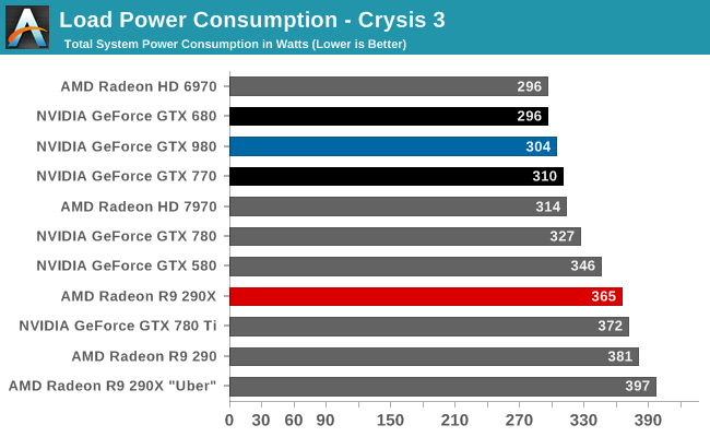
Because, as we have learned, that is the average power consumption when the card isn't boosting... aka at the base clock.

165w Nvidia Maxwell TDP = ~180w average TDP = ~200w realworld TDP

I don't know about you but I personally don't expect a 165w TDP card to be inbetween a 195w GTX680 and a 230w GTX770.

67754.png
 
Last edited:
In the new PCWorld article on FuryX, AMD cites 100mhz overclock as some big deal...1050 to 1150 on the core....doesn't seems much to me?

Nicely, AMD own numbers falls inline with what i asked earlier...1150mhz FuryX vs 1300mhz 980Ti, who will win?
 
Back
Top