
You are using an out of date browser. It may not display this or other websites correctly.
You should upgrade or use an alternative browser.
You should upgrade or use an alternative browser.
Speculation and Rumors: Nvidia Blackwell ...
- Thread starter pharma
- Start date
Not according to this:They can refresh with B200 on 3nm anyways which is next year apparently.
Bondrewd
Veteran
MI200 already did that just fine (if you remember that the OAM MI100 was shitcanned for reasons).Seems impossible to jam over 1400mm^2 of the same silicon into the same power envelope
Clock it lower and that's all.
MI200 already did that just fine (if you remember that the OAM MI100 was shitcanned for reasons).
Clock it lower and that's all.
Still got to perform at those lower clocks though. Perf/w will be the key thing to watch.
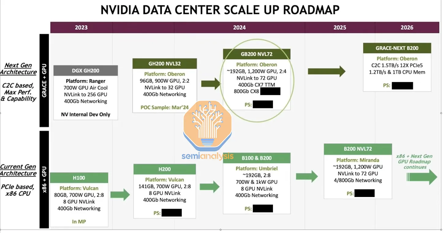
B200 seems to be the same chip as B100 but with 1000W TDP instead of 700W.They can refresh with B200 on 3nm anyways which is next year apparently.
Bondrewd
Veteran
Yea, that's the trick with spamming twice the Si.Still got to perform at those lower clocks though. Perf/w will be the key thing to watch.
They're both kilowatt, no worries.B200 seems to be the same chip as B100 but with 1000W TDP instead of 700W.
700W B100 is meme/10.
DavidGraham
Veteran
An important information, seems NV was secretly doing compute chiplets years ago (since A100).
Seems gaming Blackwell is going the same route.
Seems gaming Blackwell is going the same route.
Impossible. Everyone knows that Nvidia can't do chiplets.I thought everyone knows this because nVidia has written and spoke about it four years ago...
DavidGraham
Veteran
This might explain why B202 is rumored to be 512 bit, it's dies connected together, appears as one huge gaming die. It explains why it's called B202 and not B102.
It's GB202 and they all are GB20x since they are "Blackwell 2.0" whatever that means in comparison to "1.0". Probably that they are on N3.This might explain why B202 is rumored to be 512 bit, it's dies connected together, appears as one huge gaming die. It explains why it's called B202 and not B102.
Bondrewd
Veteran
The latter.Is Blackwell just a wider Hopper or have there been architectural changes?

Frenetic Pony
Veteran
The interlink bandwidth sounds incredible, but otherwise "two H100s stapled together (in terms of compute resources) but without double the HBM" isn't exactly what I was expecting out of Nvidia.

NVIDIA Blackwell GB202 Gaming GPUs To Utilize TSMC 4NP Node, Significant Improvement To Cache & SM Throughput
NVIDIA announced its Blackwell GPUs for AI and now eyes are all set on its gaming parts which are rumored to feature the same TSMC 4NP node.
It was previously expected that NVIDIA was going to leverage the TSMC 3nm process node for the gaming chip but that plan has seemingly changed as Kopite7kimi now states both Blackwell AI Tensor Core and Gaming GPUs to be fabricated on a very similar process node. Just a few hours ago, we came to know that NVIDIA will be using TSMC's 4NP node, a variation of the 5nm node that was already used for Ada Lovelace and Hopper GPUs.
It is stated that the new process node will allow a 30% increase in transistor density which can lead to higher performance gains but the actual efficiency advantages are yet to be explained. TSMC doesn't explicitly state the 4NP process node anywhere on its webpage. They only mention N4P & which is also mentioned as an extension of the N5 platform with an 11% performance boost over N5 and a 6% boost over N4.
...
He also mentions that the GB203 GPU, the next in the Blackwell Gaming GPU lineup, will be half of the GB202, similar to AD102 and AD103 GPUs. This will lead to a huge disparity in performance if NVIDIA equips the next 90-series cards with GB202 and the 80-series cards with GB203. The biggest question is whether NVIDIA will utilize MCM (Multi-Chip-Module) packaging for its Blackwell Gaming GPUs or keep them monolithic for now. Given the increasing costs and yield issues associated with GPU/chip development, the chiplet route is indeed the way of the future & AMD's Radeon division has already embraced it.
B100 doubled the HBM3 memory from H100 and has 2.4x more bandwidth. It is basically a H100 NVL with 8TB/s instead of 600GB/s (NVLink).The interlink bandwidth sounds incredible, but otherwise "two H100s stapled together (in terms of compute resources) but without double the HBM" isn't exactly what I was expecting out of Nvidia.
.jpg)
NVLink & NVSwitch for Advanced Multi-GPU Communication
The Most Powerful End-to-End AI and HPC Data Center Platform.
www.nvidia.com
NVLink Switch Generational comparison
| First Generation | Second Generation | Third Generation | NVLink Switch | |
|---|---|---|---|---|
| Number of GPUs with direct connection within a NVLink domain | Up to 8 | Up to 8 | Up to 8 | Up to 576 |
| NVSwitch GPU-to-GPU bandwidth | 300GB/s | 600GB/s | 900GB/s | 1,800GB/s |
| Total aggregate bandwidth | 2.4TB/s | 4.8TB/s | 7.2TB/s | 1PB/s |
| Supported NVIDIA architectures | NVIDIA Volta™ architecture | NVIDIA Ampere architecture | NVIDIA Hopper™ architecture | NVIDIA Blackwell architecture |
NVLink Generational comparison
| Second Generation | Third Generation | Fourth Generation | Fifth Generation | |
|---|---|---|---|---|
| NVLink bandwidth per GPU | 300GB/s | 600GB/s | 900GB/s | 1,800GB/s |
| Maximum Number of Links per GPU | 6 | 12 | 18 | 18 |
| Supported NVIDIA Architectures | NVIDIA Volta™ architecture | NVIDIA Ampere architecture | NVIDIA Hopper™ architecture | NVIDIA Blackwell architecture |
Last edited:
It's honestly super un-exciting. Per processor, the improvements really aren't that big at all. They must be quite assured in their current lead given this is supposed to be their new flagship for the next two years.The interlink bandwidth sounds incredible, but otherwise "two H100s stapled together (in terms of compute resources) but without double the HBM" isn't exactly what I was expecting out of Nvidia.
This new era of 'more performance by using more silicon' is gonna kinda suck.