
You are using an out of date browser. It may not display this or other websites correctly.
You should upgrade or use an alternative browser.
You should upgrade or use an alternative browser.
Nvidia GT300 core: Speculation
- Thread starter Shtal
- Start date
- Status
- Not open for further replies.
Well, so it has an extra chip between itself and the memory, but isn't that the same situation as a northbridge with memory controller?
Yes, it does. But I guess this had to be done to address the ultra-large server market.
TimothyFarrar
Regular
Getting back to the multiple-program-multiple-data/MPMD (not MIMD) : So GT200 and prior compiled VS(+GS)+PS into one "program"? This "program" might mean that shared memory block size would be the union of shared memory block size used by the VS(/GS)/PS shaders so that the hardware could dynamically switch between VS and PS entry points of the program depending on geometry/load balancing needs. With GT300 we expect to be able to run more than one "program" simultaneously.
I went back a read through Theo's term mangled comments again because I didn't get what he ment before when saying "cluster organization is no longer static. The Scratch Cache is much more granular and allows for larger interactivity between the cores inside the cluster." Seems as if he used the same term "sratch cache" when talking about G80 arch compared to ATI previously not having shared memory. So "sratch cache" literally means "shared memory".
Shared memory already provides fine granularity accesses, unless he is saying that bank conflicts would be lower (which wouldn't make any sense at all). Also thread2thread interactivity or warp2warp (in the same block) interactivity is also fully granular (through shared memory). So he must be attempting to describe something else,
What if shared memory was now shared across four 8-wide SIMD multiprocessors in a cluster (moving up from 3 multiprocessors/cluster in GT200, to fit the 512 "core" rumor)? So you'd have 32KB*4 or 128KB of banked shared memory per cluster.
It won't be meaningful then. I mean what's the point of adding another level in thread & memory hierarchy which has no useful benefit what soever. If you wanted inter block communication, why would you limit it to 4 blocks only? This super block would allow more threads to communicate within itself, but what happens to inter superblock communication. They may make shared memory more useful, "featureful", but if all that is to be achieved with this proposal is limited inter block communication (short of full any-block-to-any-block communication), then why not just make the max block size larger?
TimothyFarrar
Regular
It won't be meaningful then. I mean what's the point of adding another level in thread & memory hierarchy which has no useful benefit what soever. If you wanted inter block communication, why would you limit it to 4 blocks only? This super block would allow more threads to communicate within itself, but what happens to inter superblock communication. They may make shared memory more useful, "featureful", but if all that is to be achieved with this proposal is limited inter block communication (short of full any-block-to-any-block communication), then why not just make the max block size larger?
What you are bringing up is exactly the type of thing I'm wondering about. Really I'm just attempting to understand what Theo is attempting to say
")
BTW, I'm not saying that there would be another level, just a larger shared memory (ie larger shared memory register file) and more than one multiprocessor attached to the shared memory. The 4* comes from 4 multiprocessors not blocks. Blocks could still use a variable amount of memory (kind of wondering exactly how they would intend to handle the dynamic allocation however!).
Also not that this would be DX11 CS API accessible (maybe CUDA 3.0 only), you'd still have the 32KB limit per block in DX11 CS. However I'm wondering if they could perhaps make use of this larger multiprocessor shared memory for cross shader communication in parts of the DX11 pipeline?
assuming that InterlockedAdd() supports floating point in DX11 (which I'm not 100% sure of)
It does not. Int and uint only for all atomics.
It would be a shame if these atomics are not floating point.
Well, we don't have any floating point atomics on CPUs either. A floating point InterlockedAdd wouldn't make much sense anyway since floating point adds are order dependent, which kind of breaks the usage model of it. Floating point InterlockedMin() and InterlockedMax() on the other would make sense and be useful.
Well, so it has an extra chip between itself and the memory, but isn't that the same situation as a northbridge with memory controller?
The difference is that there is only one client. Specially important for 8+ socket machines. Also the protocol will be much simpler, you are only abstracting a memory access, not implementing a full blown SMP CPU bus.
Jawed
Legend
I've realised that the longest sides on Nehalem-EX can't be more than around 30mm - similar to the longest sides on Larrabee. That would mean that SMI on Nehalem-EX is providing what seems to be a 512-bit DDR interface in ~same perimeter as RV770's 256-bit GDDR5.I haven't worked out yet what the effective DDR bus width per chip is or how this compares with the size of the DDR interfaces on Nehalem.
But there's no doubt a question on the actual bandwidth...
Jawed
Jawed
Legend
One program is a peculiar idea. If anything I'd say that only one type of kernel could run on a given multiprocessor at any one time.Getting back to the multiple-program-multiple-data/MPMD (not MIMD) : So GT200 and prior compiled VS(+GS)+PS into one "program"? This "program" might mean that shared memory block size would be the union of shared memory block size used by the VS(/GS)/PS shaders so that the hardware could dynamically switch between VS and PS entry points of the program depending on geometry/load balancing needs. With GT300 we expect to be able to run more than one "program" simultaneously.
But even that I'm dubious about. I think patent documents referred to allocated registers in the register file from both top and bottom, e.g. vertices from the bottom and pixels from the top (I think ATI does this, but don't remember it being specifically mentioned for NVidia, now I think about it).
One of the remaining problems I have with G80 architecture is the scheduling of work within a cluster. It's my suspicion that scheduling is common to the cluster (i.e. there is one scoreboard of some type that rules in the creation of warps, the progress of instruction pages, issue to TMUs), which is how TMUs can be shared across multiprocessors.I went back a read through Theo's term mangled comments again because I didn't get what he ment before when saying "cluster organization is no longer static. The Scratch Cache is much more granular and allows for larger interactivity between the cores inside the cluster." Seems as if he used the same term "sratch cache" when talking about G80 arch compared to ATI previously not having shared memory. So "sratch cache" literally means "shared memory".
Shared memory already provides fine granularity accesses, unless he is saying that bank conflicts would be lower (which wouldn't make any sense at all). Also thread2thread interactivity or warp2warp (in the same block) interactivity is also fully granular (through shared memory). So he must be attempting to describe something else,
He could be talking about DWF.
The bigger you make it the slower it gets. But if you want some kind of on-die variably sized inter-kernel queuing then maybe sacrificing some shared memory is part of the trick - but that would only be able to feed the per-cluster scheduler if it was flat as viewed by the cluster scheduler. But that kind of flatness shouldn't necessitate making it literally flat.What if shared memory was now shared across four 8-wide SIMD multiprocessors in a cluster (moving up from 3 multiprocessors/cluster in GT200, to fit the 512 "core" rumor)? So you'd have 32KB*4 or 128KB of banked shared memory per cluster.
Jawed
Jawed
Legend
I suppose matrix multiplication has the same problem.Well, we don't have any floating point atomics on CPUs either. A floating point InterlockedAdd wouldn't make much sense anyway since floating point adds are order dependent, which kind of breaks the usage model of it.
There was a paper recently that moaned about having to use integer format for atomic add - I think they resorted to fixed-point.
Any kind of reduction kernel also inherently suffers the same order-dependent-precision problem - and reductions in Brook+ for example support floating point.
Jawed
I guess you can start with Nehalem-EX's SMB. That's real, it's working and it appears to be doing exactly what this patent proposes.
I'm curious if NehalemEX's design has been shifted to completely abandon FB-DIMMs this late in the game, or rather that the SMB is a somewhat lateral move where Intel transplanted the on-board buffer chip on the DIMMs to the motherboard.
In which case, as far as the FB-DIMM controllers on Beckton are concerned, nothing has changed at all, and the SMB might be a somewhat elaborated hardware kludge to match silicon that is so far along with market forces that have dispensed with the memory technology the chip targets.
I have already pointed out that the Nvidia patent looks incredibly similar to FB-DIMMs, and I still do not see what was novel about it.
The hub chips are useful if Nvidia forsees that it will be heavily pad limited, or that it sees that it will continually be on the losing end of memory technology transitions.
Given that GPU boards are not expandable, and do not support multi-drop buses, a large part of the argument for the hub chip is irrelevant in this context.
Jawed
Legend
That's how the patent application paints it - so really it's a question of whether GDDR5 surmounts those eventualities.The hub chips are useful if Nvidia forsees that it will be heavily pad limited, or that it sees that it will continually be on the losing end of memory technology transitions.
But GPU chips are required to support multiple configurations, even if they're static once sold.Given that GPU boards are not expandable, and do not support multi-drop buses, a large part of the argument for the hub chip is irrelevant in this context.
Jawed
That's how the patent application paints it - so really it's a question of whether GDDR5 surmounts those eventualities.
GDDR5 helps with the bandwidth problem, which could reduce the need for more pads.
If the problem is that Nvidia can't time GDDR design cycles, there's something else wrong that the hub wouldn't be able to compensate for. (GDDR5's planned lifetime seems to be longer, so this might also be less urgent)
A hub would make ECC easier to implement, since it would otherwise require additional memory pads on the GPU for each memory controller to contact an extra chip, which at GT200 die sizes means there is no additional room with the reticle limit.
There's also the chance that such contacts might also go unused, even if there were room, though I wonder if there would be other ways to get around that (a bonus extra channel or two in non-ECC mode?)
The hub is a really roundabout way of getting to that point.
Simpler would be to just design the chip to be smaller in the first place, then be rewarded with even more space to be awesome when ECC is added. AMD has that option, possibly.
But GPU chips are required to support multiple configurations, even if they're static once sold.
Part of the benefit for having the buffer chip converting a parallel DRAM interface to a serialized bus was the electrical difficulties inherent to placing many parallel buses or many loads operating at speed on many DIMM slots.
Soldered chips don't have the same electrical problems that a removable DIMM has with electrical discontinuities, and the capacity of GPU boards is miniscule compared to what a fully loaded server socket might sport.
Some of the additional signalling features GDDR5 have actually distributed some of AMB features out to the DRAM chips.
One thing that still remains is that a hub chip can abstract away changing memory standards, which could save costs and hide the inflexibility of on-die CPU memory controllers getting stuck with last year's memory technology and making the CPU less future-proof.
GPU memory, being soldered on, makes this a given already.
Nvidia might save some design costs, though this isn't a compelling argument for those that actually build and sell the boards.
Any kind of reduction kernel also inherently suffers the same order-dependent-precision problem - and reductions in Brook+ for example support floating point.
Sure. It's usually not so important which order you choose, but it's important that a specific order is chosen and that you stick to it to get consistent results. If you're doing a reduction for instance for HDR exposure and the order in which pixels are added together changes randomly from frame to frame depending on threading and timing you could get subtle flickering as a result.
spacemonkey
Newcomer
it's kinda hard to see in this die photo, does anyone have higher rez?I've realised that the longest sides on Nehalem-EX can't be more than around 30mm - similar to the longest sides on Larrabee. That would mean that SMI on Nehalem-EX is providing what seems to be a 512-bit DDR interface in ~same perimeter as RV770's 256-bit GDDR5.
But there's no doubt a question on the actual bandwidth...
Jawed
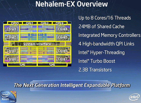
edit: answered my own question =)
on page 6 of http://download.intel.com/pressroom/pdf/nehalem-ex.pdf
Last edited by a moderator:
I can inform you that current A1-samples are clocked at 700/1600/1100 MHz. So they come to impressed 2,457 Gigaflops and 281 GB/s memory bandwidth.
It is nice, is not it?
Source: Hardware-Infos
If they be that far along, why aren't they showing them off this week, or is it planned to happen after ATI does theres to one up them?
If correct, then there are two good reasons:
1. Volume. Takes time.
2. Hard launch. Takes coordination and planning.
Right now TSMC has problems getting one chip out in volumes (RV740) I'm hard pressed to see anything coming out in big volumes from both IHV's.
How can nVidia get their monstrous GT300 out the door in time when they can't even properly work with their die shrunk G8X's?
If correct, then there are two good reasons:
1. Volume. Takes time.
2. Hard launch. Takes coordination and planning.
Ahhh.... I hate you, I just spend like an 1.5h at the website in your sig...
Ahhh.... I hate you, I just spend like an 1.5h at the website in your sig...
lol, me too, the escalator one cracked me up!
- Status
- Not open for further replies.