
The original slew of "R520 = 32pipes" rumors have their origin in R520 die size. It has been know for some time that it would be rather large ( > NV40), leading some to conclude that it will indeed be 32-pipes. As it stands, R520 is the biggest graphic chip to date - at 320Mts, its twice the size of its predecessor. So, what are some of the key factors contributing to this massive transistor count increase? Memory controller? SM3 logic? Larger Caches?
You are using an out of date browser. It may not display this or other websites correctly.
You should upgrade or use an alternative browser.
You should upgrade or use an alternative browser.
R520 die size and transistor count redux
- Thread starter Geeforcer
- Start date
I'm willing to bet that the #1 contributing factor is the extra register space required in order to have many threads in-flight at once.Geeforcer said:The original slew of "R520 = 32pipes" rumors have their origin in R520 die size. It has been know for some time that it would be rather large ( > NV40), leading some to conclude that it will indeed be 32-pipes. As it stands, R520 is the biggest graphic chip to date - at 320Mts, its twice the size of its predecessor. So, what are some of the key factors contributing to this massive transistor count increase? Memory controller? SM3 logic? Larger Caches?
Take a look at page 9.
Yes, they had a bit of a ring sting (engineers had too many curries...") )
)
)That would seem really, really odd, considering the "Ring bus" gains its high clockability from having the traces around the outer edge of the die. How, then, can the center be directly related to this bus?
I'm willing to bet that that center block is cache memory for local register storage.
I'm willing to bet that that center block is cache memory for local register storage.
I sent the link with the die photo to someone who really knows how a die floorplan looks like and even without saying a thing the first he answered was that the memory controller was in the center. PR slides showing 'rings' and stuff are completely misleading. In fact I doubt it's a ring but more likely some kind of 'square' so bus traces can run either horizontal or vertical. And of course it would have better latency if it is an inner ring rather than an outer ring. Look at how the four blocks are arranged (and the additional block at the bottom right side must be video related) around the center. I expect the memory controller to have large buffers and thus you are also right that it has a lot of memory there.
The ring is only the method by which the returned data travels to the requesting client - the memory controller is still at the center of the device, its just that the by placing the data return path around the chip there isn't a massive density around the controller (mainly only the clicne request connections and the controller connections to the ring stops).
It may be related to the memory controller, but it still looks an awful lot like cache. I don't know of anything else within the chip that could possibly look that uniform over such a large area.Dave Baumann said:The ring is only the method by which the returned data travels to the requesting client - the memory controller is still at the center of the device, its just that the by placing the data return path around the chip there isn't a massive density around the controller (mainly only the clicne request connections and the controller connections to the ring stops).
Chalnoth said:It may be related to the memory controller, but it still looks an awful lot like cache.
No it is clearly logic (boost the gamma a bit and you can see that the area is not really uniform), eight identical blocks.
Jawed
Legend
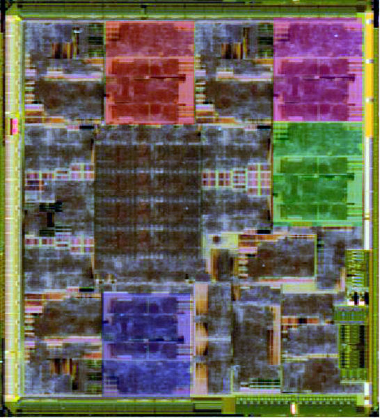
I've marked out what I suppose are the pixel shader ALUs and texture pipes. The blue one is "upside down". Next to it is a unit which is also found next to the red and magenta areas. The green area doesn't have such a partner.
Those marked areas are 28% of the die, by the way - roughly.
Ah well...
Jawed
Yes it does, well, part of it at least. Just down and to the left of the green area.Jawed said:I've marked out what I suppose are the pixel shader ALUs and texture pipes. The blue one is "upside down". Next to it is a unit which is also found next to the red and magenta areas. The green area doesn't have such a partner.
Jawed
Legend
Yeah, you guys are right, most of that stuff by the red, magenta and blue areas is repeated near the green.
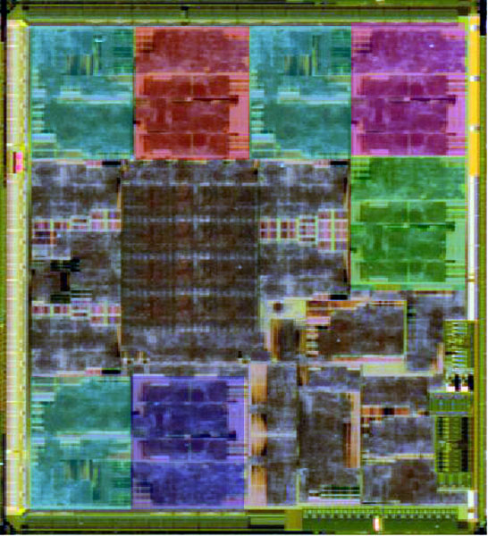
Though not quite all of it. That is the problem I'm having. Of course, it's a bit naive to lump a perfect rectangle together as a functional block.
Anyway, it's mildly diverting.
Now, who can spot the 8 vertex shaders?
Jawed
Though not quite all of it. That is the problem I'm having. Of course, it's a bit naive to lump a perfect rectangle together as a functional block.
Anyway, it's mildly diverting.
Now, who can spot the 8 vertex shaders?
Jawed
Jawed
Legend
The other thing is, I think this prolly explains why ATI has been so eager to build a unified shader for so long.
If the scheduler and the out of order scheduling of lots of small batches is quite costly to implement (lots of memory for registers), then it makes sense to unify the shader hardware that performs vertex/fragment shading and make most use of the scheduler's "overhead".
Jawed
If the scheduler and the out of order scheduling of lots of small batches is quite costly to implement (lots of memory for registers), then it makes sense to unify the shader hardware that performs vertex/fragment shading and make most use of the scheduler's "overhead".
Jawed


Mmm vpu porn *drool*Jawed said:Yeah, you guys are right, most of that stuff by the red, magenta and blue areas is repeated near the green.
Though not quite all of it. That is the problem I'm having. Of course, it's a bit naive to lump a perfect rectangle together as a functional block.
Anyway, it's mildly diverting.
Now, who can spot the 8 vertex shaders?
Jawed
Love_In_Rio
Veteran
How many transistors do you supposse would involve the addition of 2 more pixel quads ? Possible with 90 nm ?
Similar threads
- Replies
- 3
- Views
- 4K
- Replies
- 70
- Views
- 19K
- Replies
- 125
- Views
- 17K
- Replies
- 0
- Views
- 1K