AMD Radeon RDNA2 Navi (RX 6500, 6600, 6700, 6800, 6900 XT)

Following the floorplan, 1 32-bit PHY and Memory controller takes the area of approximately 3.4 slices of L3, i.e. you can replace 32-bit GDDR6 bus with 13.6 MB of cache.
Assuming linear scaling of SRAM and lack of the 32-bit PHY scaling, it would be 5.4 slices of L3 or 21.6 MB of cache per 32-bit GDDR6 bus on TSMC 5 nm, so they can pack up to 172 MB of L3 in the same die footprint (~184 MB assuming MCs will shrink too).
The bottom line is that sram should be much more attractive on 5 nm.
 
Last edited:
I expected (based on the note by AMD, that IC is somewhat based on Zen's L3) density of about 1 MB per mm², but it seems they achieved much higher value. It's 8 MB per 4,9 mm², so 1,63 MB per mm². IC of Navi 21 (128 MB) should take only 78,5 mm². Navi 21 without the IC would need additional ~256bit bus to reach bandwidth comparable to RTX 3090, which would cost at least 62,2 mm² of silicon (probably more, I have not included longer infinity fabric etc.), more complex packaging and more complex PCB.
 
Does the RTX 3090 actually "need" that much bandwidth? By extension would a hypothetical 6900XT "need" what I assume you're saying would be a 512 bit bus running GDDR6 14/16 Gbps? I'd wager, at least for the main target use cases, a hypothetical 384 bit bus with GDDR6 16Gbps would be "enough" as a hypothetical alternative to IC. Also I'd wonder if a 512 bit bus is even implementable, especially at 14Gbps+, given technical constraints.

This is more of an Nvidia aside, but I've been skeptical of how much Nvidia actually benefits from GDDR6X. At this point I wonder if it's usage into end products involved other market factors than actual technical considerations for said products. Also to some extent whether or not at least the current (first) gen memory and/or memory controller is actually underperforming projections (including actual effective bandwidth due to error rates/thermals).

This even extends back to GDDR5X and also to some extent HBM with AMD. It seems like these forays away from GDDR for consumer cards have historically been rather questionable in terms of the actual gains.
 
N5 SRAM is 1.3x in vacuum and close to nil in reality.
Didn't watch for sram scaling closely - too many sources which point into different directions, but sad if true.
SRAM has always been the highest density cells, but it seems the sram scaling has hit certain walls, which logic hasn't hit yet due to much lower density.
Anyway, any scaling relative to something that doesn't scale at all would make sram more attractive.

The reality is that SRAM is moving as far away from logic spam nodes as possible.
Depends on what kind of sram it is, have a hard time imagining registers and SIMD caches move anywhere anytime soon.

Navi 21 without the IC would need additional ~256bit bus to reach bandwidth comparable to RTX 3090, which would cost at least 62,2 mm² of silicon (probably more, I have not included longer infinity fabric etc.), more complex packaging and more complex PCB.
There are lots of moving parts, but frankly any chip maker would love to move costs towards parts he sells, which I guess what IC does. Given that console makers have not adopted it, it's probably not the most cost efficient overall board configuration at least in case of consoles.
 
Does the RTX 3090 actually "need" that much bandwidth? By extension would a hypothetical 6900XT "need" what I assume you're saying would be a 512 bit bus running GDDR6 14/16 Gbps? I'd wager, at least for the main target use cases, a hypothetical 384 bit bus with GDDR6 16Gbps would be "enough" as a hypothetical alternative to IC. Also I'd wonder if a 512 bit bus is even implementable, especially at 14Gbps+, given technical constraints.

This is more of an Nvidia aside, but I've been skeptical of how much Nvidia actually benefits from GDDR6X. At this point I wonder if it's usage into end products involved other market factors than actual technical considerations for said products. Also to some extent whether or not at least the current (first) gen memory and/or memory controller is actually underperforming projections (including actual effective bandwidth due to error rates/thermals).

This even extends back to GDDR5X and also to some extent HBM with AMD. It seems like these forays away from GDDR for consumer cards have historically been rather questionable in terms of the actual gains.
Has any high end Nvidia GPU for the last several generations ever benefited more from memory OC over core OC? From my memory it’s a no. Are RT cores bandwidth hungry?
 
There are lots of moving parts, but frankly any chip maker would love to move costs towards parts he sells, which I guess what IC does. Given that console makers have not adopted it, it's probably not the most cost efficient overall board configuration at least in case of consoles.
AMD stated, that IC was developed because of mobile segment. It makes sense. Narrower bus allows AMD to get to mobile devices. 256bit for high-end is not a problem, 512bit would be. 128bit for mainstream is not a problem, 256bit isn't so great etc.
 
SRAM has always been the highest density cells, but it seems the sram scaling has hit certain walls
Cells scale but only with moar assist circuitry aka real area scaling dies.
have a hard time imagining registers and SIMD caches move anywhere anytime soon
SoIC+ is like 2026 and has sub-micron pitches so maybe then.
Given that console makers have not adopted it, it's probably not the most cost efficient overall board configuration at least in case of consoles.
Consoles still have to pay for them memory chips to hit their capacity points so plastering SRAM to sell less memory chips is utterly counterproductive there.
 
Has any high end Nvidia GPU for the last several generations ever benefited more from memory OC over core OC? From my memory it’s a no. Are RT cores bandwidth hungry?

I have a vague recollection of a few GPUs with close to pseudo linear (as in at least around 1:2 or better) scaling at higher resolutions from both AMD and Nvidia in past (although I can't specifically recall which off hand). However in general they've been paired with what would be considered adequate more than adequate (especially for the "cutdown" SKUs) memory bandwidth.

My understanding is that ray tracing can be memory hungry in certain scenarios. However in general I haven't seen much real results from current games that show much divergences between non ray trace scenarios. For instance the 3070 vs 3070ti performance delta seems fairly proportionate in either scenario. It's worth noting that the Quadros (although this was likely dictated by capacity) are strictly GDDR6 only, despite that their workloads are likely more compute or ray trace (for rendering) heavy.

A GDDR6 16Gbps RTX 3090 would likely be slower, but just not anywhere near to the extent the nearly 20% loss in bandwidth would suggest. With something like the 6900XT I'd wondering if a 384bit with no IC version would actually be faster at 4k (or maybe the same) but slower at 1080p than what we have now, just with higher power draw.

I just wonder if there was more to the decision such as existing commitments with Micron possibly even extending as far back as the GDDR5X deal. Or things such as being able to secure enough GDDR6 contracts (as Nvidia did release slightly earlier and has several times more volume than AMD).
 
Speaking of memory, the 6900 XT LC, that (formerly) OEM thing, has 18 Gbps GDDR6.

With that comes my question: how well does RDNA2 scale with VRAM speeds considering it's got IC in the GPU die itself that should make it less dependent on memory speeds.
 
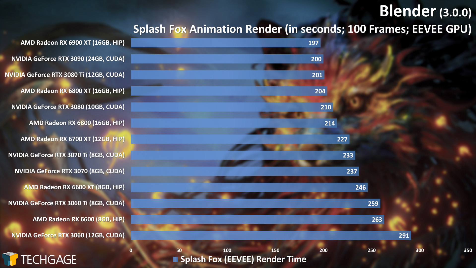
In the more complex EEVEE Blender project it appears AMD have gained some ground as it only has 40% average GPU usage. Not that it makes up for all other loads, like viewport performance.

Blender-3.0.0-EEVEE-Render-Performance-Splash-Fox.jpg
 
Last edited:
raw performance makes difference.

Raw performance doesn’t explain most of the results with the 3070 and 3060 rubbing shoulders with a 6900 XT. The API is likely playing a significant role. Maybe they are using CUDA tricks that aren’t available in HIP yet.

Eevee in particular is interesting because it’s an OpenGL rasterizer so it’s really bizarre that a vanilla 3060 is 30% faster than a 6900 XT. There’s clearly more than raw performance at play there.
 
editing previous post with new attachment gone wrong, here it is:
Raw performance doesn’t explain most of the results with the 3070 and 3060 rubbing shoulders with a 6900 XT. The API is likely playing a significant role. Maybe they are using CUDA tricks that aren’t available in HIP yet.

Eevee in particular is interesting because it’s an OpenGL rasterizer so it’s really bizarre that a vanilla 3060 is 30% faster than a 6900 XT. There’s clearly more than raw performance at play there.
Yeah, this alone makes total sense:

RX6k.PNG
 
Low load might come because of small tile size, if it's appliable to HIP version of the renderer. If defaults to very small CPU-friendly values (32x32 or 64x64, don't remember it precisely) and if you increase it to something like 320x200 it'd be literally several times faster than it usually is. I've rendered Schoolroom and Ryzen logo on my Vega56, it literally goes from one minute to less than 10 seconds with some tile size tweaking (GPU load (in watts) increases correspondingly)
 
Back
Top