AMD CDNA Discussion Thread

MI300, CDNA 3. Sharing memory & IO for CPU and GPU. 24 Zen 4 cores, 128GB HBM3, 146B transistors. 3D stacking multiple chiplets on a base die - 9x 5nm chiplets 3D stacked on 4x 6nm chiplets. Claim 8x AI Tflops and 5x AI perf/w (Tflops/w) vs MI250X - specified Tflops not TOPs, 3Pflops FP16/Bfloat16 not lower precision formats (Int8/4)*? "Sampling to customers shortly" and coming to market 2H 2023

*MI250X Int8/4 rates are the same as FP16/Bfloat16, 383Tflops/TOPs so they could have a "free" 2x/4x if they went full rate

 
I wonder if there are actually only 3 physical CCXes, or it's just that some cores have been disabled. Or maybe there are CCXes with < 8 physical cores. 24 Zen 4 cores is a weird number.
 
Yea you cant just reuse the standard Zen 4 chiplets for this, given they're being stacked on top of L3 cache chiplets.
 
mmm proper 3D stacked chiplets.

9x 5nm chiplets stacked upon 4x 6nm chiplets - the "asymmetry" is a head-scratcher.

3x 6nm chiplets could each have a single Zen 4, 8x core, complex atop. The final 6nm chiplet would then have 6x GPU chiplets stacked upon it?

Alternatively, 3x 6nm chiplets could each have a single Zen4, 8x core, complex atop along with 2x GPU chiplets. The final 6nm chiplet would be "IO" and have no chiplets stacked upon it.

What else?...

Chiplet bingo is fun...
 

AMD representatives showed us another MI300 sample that had the top dies sanded off with a belt sander to reveal the architecture of the four active interposer dies. There we could clearly see the structures that enable communication not only between the I/O tiles, but also the memory controllers that interface with the HBM3 stacks. We were not allowed to photograph this second sample.
 
mmm proper 3D stacked chiplets.

9x 5nm chiplets stacked upon 4x 6nm chiplets - the "asymmetry" is a head-scratcher.

3x 6nm chiplets could each have a single Zen 4, 8x core, complex atop. The final 6nm chiplet would then have 6x GPU chiplets stacked upon it?

Alternatively, 3x 6nm chiplets could each have a single Zen4, 8x core, complex atop along with 2x GPU chiplets. The final 6nm chiplet would be "IO" and have no chiplets stacked upon it.

What else?...

Chiplet bingo is fun...
Chiplet tetris is even more fun than bingo.

Building blocks
  • 1x 6nm base chiplet with 3x Zen4 CCDs on top (4 chiplets total)
  • 1x 6nm base chiplet with 2x CDNA3 GCDs on top (3 chiplets total)

AMD has the flexibility to mix and match many combinations, these are just those with 4 base chiplets.
  1. 12x Zen4 CCDs, no CDNA3 GCDs
  2. 9x Zen4 CCDs, 2x CDNA3 GCDs
  3. 6x Zen4 CCDs, 4x CDNA GCDs
  4. 3x Zen4 CCDs, 6x CDNA GCDs (matches the announced MI300, 13 chiplets total)
  5. 0x Zen4 CCDs, 8x CDNA GCDs
They could offer (and probably will announce at a later date) 1-base, 2-base, or 3-base options as well
 
Wait, but they are standard Zen4 chips.
You could reuse the general transistor-layer design, but you cant actually use the same exact chips being manufactured for Ryzen/Epyc. As Ferman points out above, at the very least there has to be differences in how they are made so they can connect to cache chips underneath.
 
You could reuse the general transistor-layer design, but you cant actually use the same exact chips being manufactured for Ryzen/Epyc. As Ferman points out above, at the very least there has to be differences in how they are made so they can connect to cache chips underneath.
That doesn't make sense to me... Why would they design the IOD in a way that they couldn't use the same chips?

A quick search and I found this article that goes into some detail.
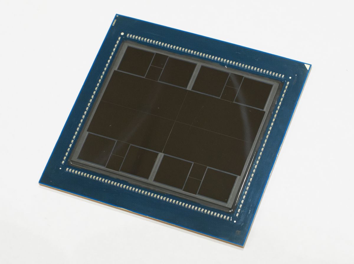
The other instance of reuse was a bit chancier. When the MI300 team decided that a CPU/GPU combination was needed, Naffziger “somewhat sheepishly” asked the head of the team designing the Zen4 CCD for the Genoa CPU if the CCD could be made to fit the MI300’s needs. That team was under pressure to meet an earlier deadline than expected, but a day later they responded. Naffziger was in luck; the Zen4 CCD had a small blank space in just the right spot to make the vertical connections to the MI300 I/O die and their associated circuitry without a disruption to the overall design.

Nevertheless, there was still some geometry that needed solving. To make all the internal communications work, the four I/O chiplets had to be facing each other on a particular edge. That meant making a mirror-image version of the chiplet. Because it was codesigned with the I/O chiplet, the XCD and its vertical connections were built to link up with both versions of the I/O. But there was no messing with the CCD, which they were lucky to have at all. So instead the I/O was designed with redundant connections, so that no matter which version of the chiplet it sat on, the CCD would connect.

The power grid, which has to deliver hundreds of amperes of current to the compute dies at the top of the stack, faced similar challenges because it too had to accommodate all the various chiplet orientations, Naffziger noted.
 
Back
Top