AMD: R7xx Speculation

Status
Not open for further replies.
b3da007.gif

http://forum.beyond3d.com/showpost.php?p=1142518&postcount=936

Is there a possibility that RV770 is surpassing as much on of GX2
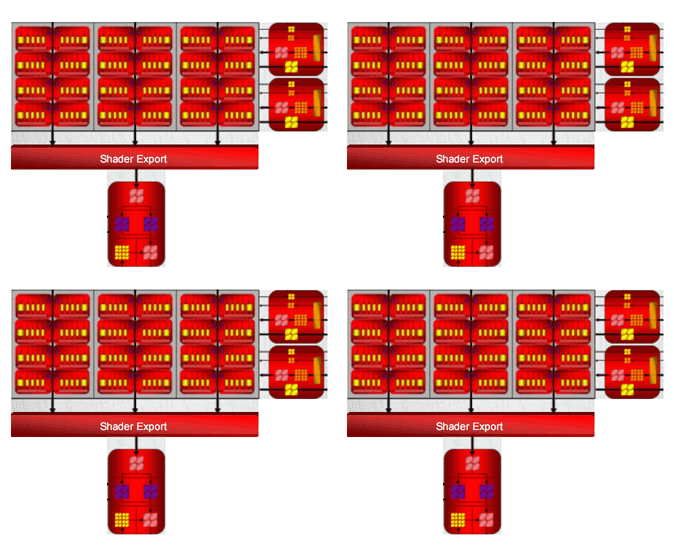
because the thread to be able to treat RV770 increases to three times
that of RV670 if this picture is true?
 
=>AnarchX: You're right, they just need to do something to make AF run faster, so perhaps they can just add texture filtering units or improve the current design somehow.
 
...The catch is, however, whether the chip really has 32 TMUs. Texturing units take up a lot of transistors and if the chip only has over 800 million, they could stay at 16.

Well, what else are you going ot use those ~134 million transistors for? I believe I've read that the ALU's in the R(v)6xx architecture are pretty densely packed and take up relatively little space per ALU. So a bump from 320 to 480 I don't imagine would take up a significant portion of that.

Are they also bumping up cache on the chip? Going back to a 1024 bit internal ringbus sounds doubtful.

From all indications Rv770 isn't a radical change from Rv670 in terms of additional supported features. It's still just DX10.1. And with Direct X's new all or nothing approach to features, it wouldn't make sense to pre-emptively add DX11 features.

Although there's always the possibility they've added some bits and bobs of things to increase the scaling or Crossfire. Or to maybe enable/assist in alternative methods of single card-multi GPU rendering other than AFR.

It wouldn't be out of the realm of possibility that a fair chunk of those addtional transisters would be dedicated to beefing up the texturing ability of the chip.

And while I'm not expecting Rv770 to be twice as fast as Rv670, I also wouldn't be surprised. After all, "IF" it more than doubles texture capability (Chip is rumored to be clocked higher after all) and has at least 1.5x (always the possibiity of 2x with increased core clock) the shader capability, then it's certainly "theoretically" possible.

So while I'm not holding my breath, I'm also not going to be surprised if it is.

Regards,
SB
 
=>AnarchX: You're right, they just need to do something to make AF run faster, so perhaps they can just add texture filtering units or improve the current design somehow.

Adding or modifying TF units would be great news; any software based sollutions rather bad news.
 
=>Silent_Buddha: From what I've heard, they'll probably make some improvements to RBEs (fixed-resolve AA perhaps?). But I don't know how much transistors would that take.
 
Any chance the R700 series is using SOI? (Assuming TSMC could provide it.) AMD would have to be looking at doing that eventually for Fusion...?
 
TSMC doesn't do SOI, so no. Seems to me that we'll never see an ATi GPU manufactured in AMD fabs, since AMD does not have the needed capacity and there are even rumours about AMD wanting to sell one of their Dresden fabs (Hector's asset light strategy ;) ). Remember Fusion doesn't have to be single die and it probably won't be. They'll just put PCIe controller on the CPU (how much transistors could 4 or 8 lanes cost?) and Fusion will be an MCM (multi-chip module - two dies under one heatspreader).
 
tomshardware said:
The RV770 GPU is equipped with a 256-bit memory controller (512-bit for the Radeon 4870 X2: The R700 represents just two RV770 GPUs slapped together).
http://www.tomshardware.com/news/ati-radeon-4800,5223.html

tomshardware said:
4870 X2 is an interesting version. AMD did not send out any specs to its partners and it is expected the board will be a bit more than just a 3870 X2 two RV770 GPUs. ATI is said to be making some changes,

I was thinking something - will Radeon 4870-X2 have single 512bit memory controller sharing two RV770 GPU's -or- two separate 256bit memory controller for each RV770 GPU that makes 512bit combine.
 
TSMC doesn't do SOI, so no. Seems to me that we'll never see an ATi GPU manufactured in AMD fabs, since AMD does not have the needed capacity and there are even rumours about AMD wanting to sell one of their Dresden fabs (Hector's asset light strategy ;) ). Remember Fusion doesn't have to be single die and it probably won't be. They'll just put PCIe controller on the CPU (how much transistors could 4 or 8 lanes cost?) and Fusion will be an MCM (multi-chip module - two dies under one heatspreader).

Well that is only step one of Fusion. The first design is supposed to be an MCM package. Then they will move to a single chip design and the final step is to integrate the GPU into the CPU pipeline. Also AMD is currently not capacity constraint. They said as much in their reacent earnings call. FAB36 is not at 100% and they have installed soom tools at FAB38 but are not activating thembecause the demand is not there.
 
=>Disharmonic: Not that I'm surprised that they don't have capacity constraints when nobody buys their slow quad-cores. Nevertheless, monolithic Fusion is such a distant future that AMD will sooner go bankrupt than launch something like that. By the way, "integrating GPU into CPU pipeline", what's that supposed to be? You mean unified arithmetic logic units supporting x86 and GPU instructions? I don't think that's possible with reasonable performance.

=>LordEC911: All sources point towards RV770 being a ~250mm2 chip with a 256bit memory interface. It's been discussed here before and it's probably not a viable option. Certainly not for AMD, who's trying to play safe in the first place. In this case it means sticking with the traditional CrossFire design and chips based on the RV670 architecture, so that the drivers will already be more or less tweaked by the time RV770 comes out. If they implemented some kind of innovative memory access technology, it would again take them half a year to cough out good drivers for it.
 
If they implemented some kind of innovative memory access technology, it would again take them half a year to cough out good drivers for it.
That's pretty much exactly I'm expecting to happen, i.e. that the two chips will have a unified memory space and it will take ages for performance to get there.

Jawed
 
That's pretty much exactly I'm expecting to happen, i.e. that the two chips will have a unified memory space and it will take ages for performance to get there.

Jawed

I agree however some benefits will be apparent from the word go, remeber indications look like a june or later release.
 
I agree however some benefits will be apparent from the word go, remeber indications look like a june or later release.

Not needing double the memory would be one! i.e. i'm assuming such a setup would allow all the memory on the card to be used as a single memory pool rather than doubling up like on current solutions.

That alone is a huge advantage IMO.
 
That's pretty much exactly I'm expecting to happen, i.e. that the two chips will have a unified memory space and it will take ages for performance to get there.

Jawed

I guess it depends which will suck more: running a game without a good driver profile for Crossfire, or one that hurts with non-NUMA memory access.

Given the close proximity of the chips and the general latency tolerance of GPUs, the NUMA penalty might not be too bad. Even CPU systems can hand-wave a certain amount of non-uniformity.

We've already seen what the lack of tuning for a driver profile can do, so let's try a new way to screw up.
 
Now that's an interesting thought. Borrow some tech from the AMD side of things to implement NUMA for the shared memory.

However, is GPU rendering actually latency tolerant enough to be able to deal with that?

Likewise if each chip has a 256 bit interface to the pool of memory it's connected to, is it possible to have a 256 bit GPU to GPU interface?

Regards,
SB
 
In a 2-socket configuration, Opteron can get by pretty well with non-uniform access, and I'd expect a GPU to be even more tolerant.

NUMA really isn't anything new, and sitting on the exact same PCB with high speed RAM would be enough for even a CPU to almost ignore the latency penalty entirely.

One problem could be that heavily used data winds up in only one memory pool.
The penalty may be more of a congestion/utilization problem, where one of the memory channels is severely underused and the other is thrashed.

There are ways to balance this. The most trivial might be some kind of interleaving of addresses, which is an option for Opteron.
 
Status
Not open for further replies.
Back
Top