Predict: The Next Generation Console Tech

Status
Not open for further replies.
The close coupling between SPEs and the RSX, which some devs are using to do some very unorthodox things, would that be difficult to emulate?

The SPEs themselves or RSX itself may be difficult to emulate if the hardware is very different.

If Sony keeps a decent connection between the cores and the GPU, the coupling isn't something hard to emulate.
If it's an SOC and a shared memory pool, it could conceivably be even easier to do.
 
Indeed.


You probably already knew/meant this, but they rather bought a license to manufacture a design. nV would never sell them the architecture IP to G7x. :p

Yes that's what I meant. :oops:

2 things I can think where issues with NV licensing that could arise are Physix and NV 3D. Not sure how many games that'd effect though and it's possible that Sony's told Devs that you're on your own with those BC-wise.
 
Too big, too power hungry, and too hot for an iteration in the performance envelope they could get elsewhere.


Additionally, IMO it would need to be NVidia to initiate and propose a new gpu. If they think they can wait until Sony comes hat in hand to them, they're going to be seriously disappointed.

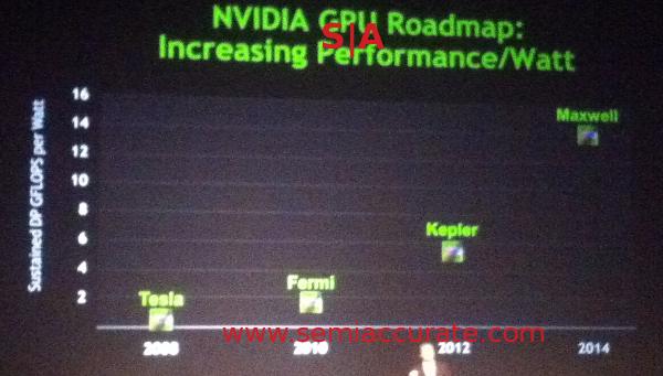
Rangers btw, I know/think you still believe Sony will go with NV and I haven't ruled NV out myself, but at this point imo they would have to come up with something really game changing (pun intended) to get serious consideration. That's certainly possible esp. when looking at this slide:

Kepler_Maxwell_Year_slip.jpg


There's obviously something up with Maxwell that cannot be explained by just a node shrink. Would NV design a nextgen gpu with Maxwell cores or something better? Would Sony accept Fermi cores with Maxwell launching about the same time? G71 vs G80 all over again? I don't think so.
So the question is, how serious is NV to stay in the console game? Are they in a position to say, take advantage of Tbyte bandwidth and deliver something unique and game changing? I'd say yes.
Then again, maybe they're getting ready to abandon highend gpu's and focus instead on HPC and SOC's. That graph afterall is about DP gflops/w.
 

Not sure why it so hard for you to type a little something about what the link is. Something like, GDC talk on procedural rendering.

Anyhow, GDC has really been focusing on mobile/indie games lately. There's alot of chaff in the wheat. Naughty Dog though has quite a few presentations this year. This one on their UC3 water tech looks promising:

http://schedule.gdconf.com/session/6482/Water_Technology_of_Uncharted

The interesting thing to me on the link is Sony presenting on DX11. That's a hint that they've been working with their nextgen tech for quite some time. And DX11 is quite interesting as well as none of their machines used DX for obvious reasons ...

Could it be? Nah! :p
 
Sony has a patent filed about a backward compatibility module (external module containing only cpu, gfx and mem, but using the console's USB, Hdd, BR-Disc, Power supply, output connectors, controllers, etc..). This should be an indication that they are considering a different architecture and that they won't do any design compromise for the sake of backward compatibility.
http://www.siliconera.com/2010/09/1...nsole-to-previous-generation-console-adapter/

I missed this tidbit.

Interesting ... I think such a solution is rather inelegant, but we've had this discussion in the BC thread.

It does indeed show that Sony is seriously thinking of dropping Cell for NG... or that they were thinking of doing a ps2 BC module! :p
 
Actually I was thinking just how feasible say, Tahiti, WOULD be in a console.

It's like 350 mm^2, similar to the ~340mm^2 Xenos+EDRAM budget.

250 watt TDP I believe (including RAM, cooling etc) just up your console budget to 300 watts (not unrealistic imo) and you're practically there. Downclock it to 800 or something to save some more.

All that's fine but the stickler is still the 384 bit memory bus there.

I'd put in a 192 bit bus, the fastest GDDR5 I could get, and call it a day and a console :p Being limited to 1080P might help the bandwidth constraints. Not sure if it's feasible but, a decent HD7970 GDDR5 overclock (not a bleeding edge one) gets you about 290 GB/s, so halve that, you'd have ~145 GB/s.
The figure is more ~ 260 sq.mm ;)
 
Not sure why it so hard for you to type a little something about what the link is. Something like, GDC talk on procedural rendering.

A lead developer of the PhyreEngine gives a talk about Advance DirectX11 Tecniques.. The link doesn't directly say he is using/learning this tecniques within Sony, but I don't think it's something he learnt just in his spare time :LOL:

Sony is definitely working on a next-generation console
 
The close coupling between SPEs and the RSX, which some devs are using to do some very unorthodox things, would that be difficult to emulate?

Mostly just emulate jump-to-self functionality on rsx, that's used heavily on spu/rsx graphics stuff. The other issue woud be to emulate the bugs of that particular revision of rsx hardware. It sure would be fascinating if all next gen consoles were amd.
 
Yes pretty much. They'd need to get libgcm running on the new gpu which shouldn't be too difficult and would be a design spec for the new gpu. That takes care of most/almost all the BC issues gpu-wise. Not sure what they expect that would need NV's permission and why it wasn't already part of the agreement with Sony already.

This assumes that libgcm is a lot higher level than it is in reality. It's in no way an abstraction layer.
 
Or maybe sony learnt from the mistake MS made :)

Sony had far more experience sourcing hardware and never would have made the mistakes Microsoft made with the first Xbox. I'm sure Microsoft's inability to renegotiate the GPU prices was a source of great humor around the SCE office in those days!

Considering the PS3 was at conception capable of playing three generations of software, I can't imagine backwards compatibility down the line wasn't a consideration accounted for in their deal with nVidia.
Until it forced Microsofts hand so they pushed forward the release of the XBox 360 before Sony were able to counter.
 
The figure is more ~ 260 sq.mm ;)

Ahh, correct. For some reason I was thinking in terms of transistors, since it had 337m with EDRAM...

And without the edram die - who's primary purpose was probably to save on paying for a fat memory bus and 8 memory chips - you're looking at 182 mm^2. That's not a big chip by enthusiast PC GPU standards.

You cant just say "without the EDRAM" as the EDRAM had ROPS and other crucial GPU parts on it, and execution logic.

Some sort of uneducated "guess" might be 200mm^2 for GPU stuff and 60mm^2 for EDRAM I would say (in Xenos). Now, there's no guarantee EDRAM will be in next box, or if there is that it will take up relatively as much die area.

Also, Xenos was indeed performance competitive with top PC GPU's in 2005.

RSX in PS3 was ~240 mm^2 according to the best I can google, without any EDRAM, as well...

You'd be looking at at least pitcairn level as to current GPU's die size, which isn't bad at all. HD7770 would already be a decent next gen console GPU and it's only 123 mm^2...

PS3 had about 470 mm^ 2 of die between Cell and RSX according to google (240/230). 360 somewhat less.

HD 6870 aka Barts is 255mm^2 according to goog, while Pitcairn supposedly "about 250".

But, G71 back in 2005 had a die of just under 200 mm^2, X1880XT tops for ATI was 288mm^2. Now top PC GPU's have gone a lot bigger, so I dont see why consoles might not follow along to some degree. Pitcairn seems like it would be doable. I also think they may use less die for CPU this time around, giving more for GPU.

The 360 GPU was ~ 180 mm^2, the CPU a touch smaller. I don't know how big the CGPU in Valhalla is, but it's probably under 200 mm^2. At no point has a "big chip" been the answer to MS's technical or cost issues and you would expect there to be a reason for that.

G71 was a shrink and tweak of G70, which was 334 mm2 and therefore utterly dwarfed Xenos. X1800XT was also much bigger as you say (288 mm2 vs 180 mm2) and the x1900XT which came out a few months later was ~ 350 mm2. Xenos really wasn't a big chip by enthusiast standards even in 2005/2006. MS could have gone much bigger but they didn't.

I doubt that adding the area of two chips together can simply give you a total die area that you can "spend" as you see fit next generation for the same cost, and so I don't see "Xenos + daughter die = PC GPU XXXX" as actually having any meaning.
 
Status
Not open for further replies.
Back
Top