https://seekingalpha.com/article/4513009-applied-materials-smic-move-another-headwind
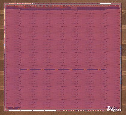
it seems that chinese semiconductor company finally moved to 7nm ( no EUV ) comparable with TSMC and
overtook the Global Foundries with their obsolete 12nm + process
it seems that chinese semiconductor company finally moved to 7nm ( no EUV ) comparable with TSMC and
overtook the Global Foundries with their obsolete 12nm + process
 and UMC is very likely to resume its 14/12nm process production soon at the request of major clients who are keenly eyeing next-generation automotive or networking chips