
You are using an out of date browser. It may not display this or other websites correctly.
You should upgrade or use an alternative browser.
You should upgrade or use an alternative browser.
AMD: Navi Speculation, Rumours and Discussion [2019-2020]
- Thread starter Kaotik
- Start date
- Status
- Not open for further replies.
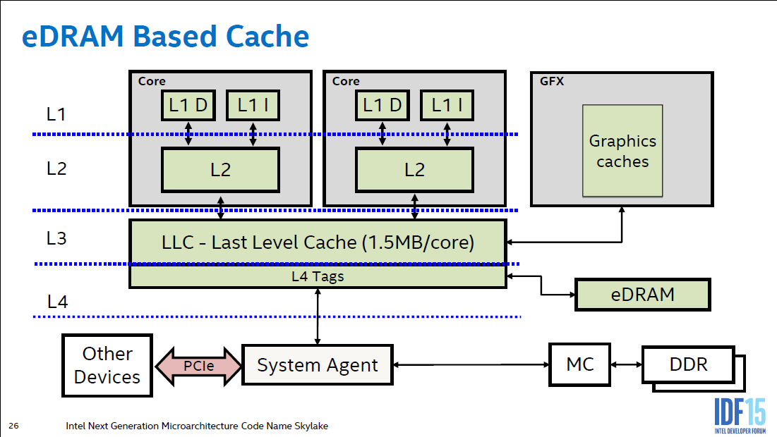
Intels Iris Pro had 128MB L4 cache, but it was on a separate die. Does this not sound very similar to what AMD is trying to do here?
Intel's Iris Pro L4 cache was trying to mitigate the extremely low memory bandwidth of the iGPU. It's an order of magnitude slower than what you'd want for a similar cache on a GPU the size of Big Navi.
https://www.anandtech.com/show/6993/intel-iris-pro-5200-graphics-review-core-i74950hq-tested/3
(Haswell, Broadwell, and Crystalwell were all the same 50GB/S bandwidth for the L4 eDRAM)
To scale that up to the 1TB - 2TB/s bandwidth you'd want to feed something like Big Navi, you'd need one heck of an interposer or EMIB.
With Zen2, even though SRAM doesn't scale as well as logic, AMD didn't dare put the enormous L3 cache on the I/O die due to the massive and power hungry inter-die connection it would have required.
Xbox One 32MB eSRAM was a close sibling, delivering double bandwidth (102 GB/s, bidirectional) than Crystalwell (50 GB/s, bidirectional). Though the former isn’t a hardware cache like the latter.Intels Iris Pro had 128MB L4 cache, but it was on a separate die. Does this not sound very similar to what AMD is trying to do here?
Can’t say for sure what AMD is going to do. But if you are in the camp of “math showing Navi 21 being suspiciously big for 80 CUs”, it would be something on-chip.
Here are some guesses I can offer:
1. 128 MB eSRAM pool (prior art: XB1) managed by “HBCC” (prior art: Vega)
2. 128 MB memory-side “L3” cache
3. 1 and 2 combined + dynamic partitioning
4. 128 MB L2 Cache
5. 4 but with L2 cache line/range locking (e.g. lock some tiles of the render target in L2 during PS?)
Last edited:
Xbox One 32MB eSRAM was a close sibling, delivering double bandwidth (102 GB/s, bidirectional) than Crystalwell (50 GB/s, bidirectional). Though the former isn’t a hardware cache like the latter.
Can’t say for sure what AMD is going to do. But if you are in the camp of “math showing Navi 21 being suspiciously big for 80 CUs”, it would be something on-chip.
Here are some guesses I can offer:
1. 128 MB eSRAM pool (prior art: XB1) managed by “HBCC” (prior art: Vega)
2. 128 MB memory-side “L3” cache
3. 1 and 2 combined + dynamic partitioning
4. 128 MB L2 Cache
5. 4 but with L2 cache line/range locking (e.g. lock some tiles of the render target in L2 during PS?)
I agree that it's almost certainly going to be on-chip. General rule of thumb for bandwidth of a cache like this is 2x memory bandwidth, so if we assume roughly 1TiB/s and work backward from there using AMD's published figures for 2nd gen Infinity Fabric on package (~9pJ/bit) - that gives you 79W consumed by the interconnect between a hypothetical off-die L4 cache and the GPU compute die. This isn't even counting the actual active power of the SRAM or eDRAM in the cache itself!
Heck, Micron's GDDR6x whitepaper was quoting 7.5 pJ/bit for GDDR6 transfers. If you needed the 1TiB/s of bandwidth you'd probably be cheaper and just as fast if not faster to just have had the 512-bit bus for the GDDR6 assuming you could fit all the PHYs on the GPU die and successfully route them to the memory packages. Doing it this way also doubles your overall VRAM capacity in addition to bandwidth, which an off-die L4 cache does not.
Well, trademarking it before would have given more clues about it being real, right?.
The same happens with PS5 and no mentions about VRS or mesh shaders. I always thought the real cause was Nvidia, as they are waiting for AMD to make its presentation, so that Sony and devs can after that be more open about PS5's tech.
I honestly think that those features just are less interesting to talk about. VRS is pretty much just what you'd expect given the D3D12 API for it with a pretty straightforward hardware implementation and mesh shaders could be interesting but haven't seen any uptake, mostly because they provide comparatively little benefit while you need to rearchitect significant parts of the rendering pipeline in the game engine. (e.g. think about what you can do with a game with mesh shaders vs. making do without. Raytracing has an obvious benefit there)
Furthermore unlike raytracing they never got the same amount of marketing as NVidia did with RTX, so there is much less of an audience and much less pressure to talk about it.
Finally, the technology for mesh shaders is mostly available on RDNA1 (with primitive shaders though those are not exposed in any API), modulo some small limitations that need to be lifted to fully implement the D3D12 API for them.
DegustatoR
Veteran
You can't make caches bigger without impacting their performance. NV had to split L2 in two parts in GA100 for example to keep it fast. L3 here is likely a better solution if you're willing to add another chip and the complex packaging into your balance sheet. Or have a die area to spare although I can't help but wonder if this is mostly for RT since one would assume that going with a wider memory bus and more execution units would result in better average performance in graphics.So if the bus width is 256, what are we expecting the bandwidth to VRAM to be? What kind of bandwidth would you need from this gpu cache to make it viable? Also, why not just make the L1 and L2 caches bigger, instead of adding another cache layer?
Well Intel use it to "cache" the super slow ddr3 ram which I think was access only by the CPU I can't remember.Intels Iris Pro had 128MB L4 cache, but it was on a separate die. Does this not sound very similar to what AMD is trying to do here?
The split in A100 seems more to tackle an horizontal scaling challenge in the interconnect, between so many SMs to so many L2 cache slices, rather than vertical scaling in the cache to stack up the capacity. L2 cache slice has been relatively tiny in comparison to CPU standards — 256KB 16-way set associative in Navi 10, for example — and argubly is less challenging than CPU cores to grow in capacity if needed be, as GPU memory systems are more latency tolerant.You can't make caches bigger without impacting their performance. NV had to split L2 in two parts in GA100 for example to keep it fast. L3 here is likely a better solution if you're willing to add another chip and the complex packaging into your balance sheet. Or have a die area to spare although I can't help but wonder if this is mostly for RT since one would assume that going with a wider memory bus and more execution units would result in better average performance in graphics.
Last edited:
Frenetic Pony
Veteran
Well, I did find something that could be relevant from their financial day this year: https://www.anandtech.com/show/1559...ckaging-for-future-products-hybrid-25d-and-3d
While it's incredibly obscure and obtuse, what it might be applicable to is this
tl;dr is that it proposes to use HBM as combination of main memory and cache. Cache for transient data that never the less needs temporary high bandwidth access, but also used as main memory for constantly accessed data to avoid tag latency penalty.
Last edited:
Love_In_Rio
Veteran
RGT says its source told him to think about PS Vita's WideIO graphic RAM in the main SOC. It was 512 bits width. Had it an interposer?.
arandomguy
Regular
RGT says its source told him to think about PS Vita's WideIO graphic RAM in the main SOC. It was 512 bits width. Had it an interposer?.
Wide I/O is a direct chip to chip interface typically done via stacking, which I believe is the case for the PS Vita.
That changed between Has-/Broadwell and Skylake.Well Intel use it to "cache" the super slow ddr3 ram which I think was access only by the CPU I can't remember.
Yes. AMD has in the past referred to "total memory on die" in marketing materials. 128MB of total memory on this die shouldn't be that hard to get to if you merely double Navi 10.
I don't know how you came up with this. The largest cache on Navi 10 is L2 and it's just 4MB.
The 45MB was total for Vega10, not Navi10. I'm pretty sure AMD never specified how much SRAM there is in Navi10, but I wouldn't be surprised if it was similar to Vega
I took a look at RDNA whitepaper and seems that everything is the same or larger, so there should be even more than 45MB of SRAM, but when I summed everything I found there it was a little over 14MB. I have no idea what else it could be.The 45MB was total for Vega10, not Navi10. I'm pretty sure AMD never specified how much SRAM there is in Navi10, but I wouldn't be surprised if it was similar to Vega
Jawed
Legend
Everyone outside of AMD has the same problem counting up all the little bits. There's buffers and function-state memories all over the place. A GPU is lots of micro-machines working together.I have no idea what else it could be.
D
Deleted member 13524
Guest
This was in reference to the PS5, not Navi 21.RGT says its source told him to think about PS Vita's WideIO graphic RAM in the main SOC. It was 512 bits width. Had it an interposer?.
Vita had WideIO on top of the SoC using through-silicon vias (TSV), so it didn't need an interposer. The PowerVR SGX543MP4 iGPU had exclusive access to it AFAIK.
It's generally the other way around with semicustom. The clients have often controlled what AMD can disclose, to the point that AMD hid that Bonaire was the same family as the current gen consoles until after they were fully disclosed/launched. I think it's more a question of how open the vendor wants to be, and that can be inconsistent.Well, trademarking it before would have given more clues about it being real, right?.
The same happens with PS5 and no mentions about VRS or mesh shaders. I always thought the real cause was Nvidia, as they are waiting for AMD to make its presentation, so that Sony and devs can after that be more open about PS5's tech.
I would wonder if the miss rate for 128MB is too high relative the the fault rate for a 4-16GB card. Miss handling would go from a hardware pipeline to what is likely a microcontroller monitoring page faults and DMA requests.1. 128 MB eSRAM pool (prior art: XB1) managed by “HBCC” (prior art: Vega)
Memory-side would impact the ISA and programming model less, and might make sense if the infinity cache name means there's a closer link to the data fabric than the anonymous L2 of the GPU. It could possibly make the concept something transferrable to other uses or products, and memory-side may make coherent memory between GPU and CPU spaces less painful.2. 128 MB memory-side “L3” cache
3. 1 and 2 combined + dynamic partitioning
Another possibility along the lines of what Intel did with its external memory is using much larger sectors than what the L2 is likely to use, to keep down the volume of cache tags.
At 128MB, I'm curious if sectors could be a significant fraction of a DRAM page in size, which could smooth over more of the read/write scheduling headaches if the data loaded is not under-utilized. For ROP or other forms of shader export, there's a good chance for using and modifying a significant portion of a DRAM page. DCC might amplify this, if small changes can propagate throughout the deltas for a ROP tile.
Something like the RBEs or shader writeback to contiguous memory could allow for more aggressive write coalescing before memory. If not explicitly managed by software, perhaps a modification to the transactions over the fabric could indicate to the cache that there's an intent to make a significant number of writes or many reads to a given sector. The cache could flag those as being recently used, with other traffic like less localized texturing potentially being relegated to a subset of ways with more turnover. I think Nvidia's L1 has something like this, where streaming data is typically serviced by a subset of the cache to avoid thrashing. ROPs and exports would have a clear hard-wired preference that could be communicated to the cache, and the aggressive coalescing in the L1/L2 pipeline might autonomously generate similar hints to another cache.
Explicit locking might be another possibility to manage on-die storage, although it may be more disruptive to the programming model.
The L2 may be in an awkward place due to its physical proximity to the key areas of the GPU, and 128MB at existing cache line lengths is a lot of lines+tags.4. 128 MB L2 Cache
5. 4 but with L2 cache line/range locking (e.g. lock some tiles of the render target in L2 during PS?)
Power-wise, I'm curious if the level of activity within the GPU's internal caches is high enough to keep a lot of that 128MB at a more active state than otherwise desired.
It would be the most transparent implementation to the rest of the system, although it's still so much cache that I wonder if AMD wouldn't want it to be a more generally applicable cache block.
Power considerations aside, if this cache is another tier in the GPU, that assumed figure reduces the amplification ratio that the L2 would provide over subsequent layers.I agree that it's almost certainly going to be on-chip. General rule of thumb for bandwidth of a cache like this is 2x memory bandwidth, so if we assume roughly 1TiB/s and work backward from there using AMD's published figures for 2nd gen Infinity Fabric on package (~9pJ/bit) - that gives you 79W consumed by the interconnect between a hypothetical off-die L4 cache and the GPU compute die. This isn't even counting the actual active power of the SRAM or eDRAM in the cache itself!
With Navi 10, it was probably in the 3-4x over VRAM. If it doesn't scale significantly, it's 1-2x of this proposed cache. If the cache and VRAM are accessed in parallel by the GPU, the L2's amplification drops below 2x if RDNA2 doesn't do something to scale it.
Interesting Patent. AMD have a Patent for Micropolygon Rasterizer. Seems they have now two rasterizer for big and for small triangles. The patent is from 2016 perfect time to appear in RDNA 2:
https://www.freepatentsonline.com/y2018/0061124.html
https://www.freepatentsonline.com/y2018/0061124.html

- Status
- Not open for further replies.