Nvidia Ampere Discussion [2020-05-14]

Probably just die size reasons. NVIDIA couldn't make the die bigger even if they really wanted to, so they'd have to cut out other parts to do it. As for why not reduce SM count to fit double ALU per SM, balance of resources is the logical answer here.
So GA102's FP32/INT32s take rather more than a trivial amount of die space compared to the INT32 version... Well, this was always my suspicion.

FP32 doesnt matter for GA100. For training they will use TF32 per default.
If it's for training and nothing else? But it has loads of FP64, which isn't for training. So FP32 doesn't matter? I would tend to agree, NVidia decided that the new tensor core was more important than anything else, but they couldn't sacrifice FP64.

Another possible scenario is that GA100 was made considerably earlier than GA10x and the updated FP32/INT h/w wasn't ready for it. We've seen something similar between Volta and Turing previously.
So could we take this to mean that the tensor core design is how NVidia now names its architectures?

If we say that Quadro/Titan/Geforce are for "prototyping" (for apps that end up on DGX) then it seems reasonable to conclude that harmonising the tensor core architecture is the most important aspect of a family of GPUs.
 
In addition to the above, Turing Tu102 still retained two FP64 "units" per SM (source for both, Nvidia Turing whitepaper, page 8). Same with GA102 (Ampere whitepaper, page 8). IIRC, the reasoning given for the 2 units per SM, were down to maintaining software compatibility. AFAIK, the smaller chips of each family get 0 FP64 units, though I may be wrong on that.

Full GV100 has 32 FP64 per 64 FP32 and full GA100 has 32 FP64 per 64FP32+64INT32. All of this without accounting for any of the Tensor core contributions.

So I do agree, it's part older design, part different goals (FP64 is a big deal in specific markets!). GA100 lacks RT cores and NVENC, for that matter, though Nvidia's specific wording was only addressing their A100 product, not the GA100.
 
So could we take this to mean that the tensor core design is how NVidia now names its architectures?
Well, there are less similarities between GA100 and GA10x than between GV100 and TU10x so... maybe?
I almost think that it's mostly "we've made these chips somewhat at the same time" thing than any technological reason. Even the same production process isn't cutting it anymore.
 
I have no GT 1030 handy, but at least 1060 still had (a few) DP-units.

Fun fact: DP-throughput on Radeon HD 5870 still beats RTX 3080. 3090 will finally beat it though.
GP104 (used for highest spec version of the GTX1060, all other GTX1060 versions had the GP106) had 4 FP64 and 128 FP32 per SM (Pascal Tuning Guide)!

That being said, I only have my laptop right now, so I'm unable to evaluate my RTX2070 (TU106) for FP64 support. IMO, it probably does include it at the same reduced level (2 per SM), though I am also curious if that extends into the TU116/117 family, since those received actual changes to the SM vs the larger Turing chips.
 
From the ixbit review (BTW very welcome to see this kind of low level feature benchmarking again, brings back memories of hardware.fr), the TMUs reportedly have been upgraded, doubling texel read speed, that is when not using filtering. These kind of TMU reads are often used in compute shaders. That is pretty cool.
Could you - again - point me to the relevant section? Or are you not talking about this ixbt-review?
 
Could you - again - point me to the relevant section? Or are you not talking about this ixbt-review?
No problem:
"In Ampere, there were also some changes in the TMU, which were modestly written in the slide along with the caching improvements: "New L1 / texture system". According to some reports, Ampere doubled the rate of texture samples (you can read twice as many texels per cycle) for some popular texture formats with point sampling without filtering - such samples are recently very often used in computational tasks, including noise reduction filters and other post-filters that use screen space and other techniques. Together with the doubled L1 cache bandwidth, this will help feed the doubled number of FP32 blocks with data."
 
Ah, I see. I was wondering if this was something they derived from their testing, because there are parts I don't necessarily agree with their conclusions. :)
 
So could we take this to mean that the tensor core design is how NVidia now names its architectures?

My impression and understanding is that these days external product codenames are as much (if not more so) a part of technical marketing than for practical internal reasons. I'd actually wonder (if given truth serum) what Nvidia (or others) actually does internally.

The likelihood is that Ampere products have much more differences, at least in terms of internal approach, than the naming suggests. However Nvidia seems to want to market their GPU designs as an unified line design wise. Whereas AMD with CDNA and RNDA it's likely they have more similarities in terms of internal approach but their new marketing approach want's a clear distinction (likely wanting to put more emphasis on their overall ecosystem including consoles).
 
eikx-3ivkayblxrvhkni.jpg


Twitter

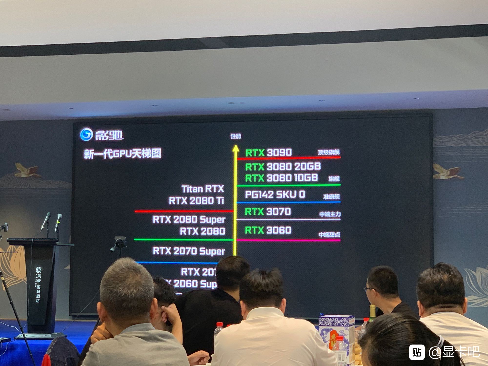
https://videocardz.com/newz/galaxs-internal-roadmap-confirms-geforce-rtx-3080-20gb-geforce-rtx-3060
 
It's not about that I arrived at different test results, it's about xbit's conclusion from their own data. Not sure, if there's something lost in translation though. For example RM's D3D10 Fire simulation, where they explicitly state, it uses one texture fetch and 130 sin/cos instructions. After the results are shown, they derive „So this time, in a purely mathematical test, the new RTX 3080 was ahead of its predecessor RTX 2080 by only 50%, which clearly indicates an emphasis on something else, and not ALU.“ while sin/cos is done by the SFUs, not the FP32-ALUs. Again, not sure, if there's something lost in translation.
 
Two YouTubers given preferred treatment over every other NDA signees.
Here's the other guy:

edit: Yes, I fully realize those are not reviews of the card, thanks.
 
Last edited:
Nice reviews, 8k60 is reality in 2020. Now DLSS and ray tracing in that mix and see how far you can come? The details and fidelity that comes available in Eternal @8k is impressive, and that at 60fps/hdr.
 
Last edited:
So it's official:

nVidia said:
For 4K gaming, the GeForce RTX 3090 is about 10-15% faster on average than the GeForce RTX 3080, and up to 50% faster than the TITAN RTX.

https://www.nvidia.com/en-gb/geforce/news/rtx-3090-out-september-24/

The leaked review was accurate.

It's also interesting that nVidia is placing the non-Titan Geforce RTX 3090 as a prosumer graphics card, as their marketing material seems to focus heavily on productivity applications.
I wonder what changed their mind on their taxonomy.
 
So it's official:


https://www.nvidia.com/en-gb/geforce/news/rtx-3090-out-september-24/

The leaked review was accurate.

It's also interesting that nVidia is placing the non-Titan Geforce RTX 3090 as a prosumer graphics card, as their marketing material seems to focus heavily on productivity applications.
I wonder what changed their mind on their taxonomy.
I think it's because there's a 12GB card in reserve against RDNA 2 (rogame has PCI IDs for a 12GB card). I mean, *maybe* the 20GB 3080s will have extra two SMs or so enabled but 20GBs will be solve at a large premium and made for prosumers or the guillable who see dat extra VRAM.
 
Back
Top