
You are using an out of date browser. It may not display this or other websites correctly.
You should upgrade or use an alternative browser.
You should upgrade or use an alternative browser.
Current Generation Hardware Speculation with a Technical Spin [post GDC 2020] [XBSX, PS5]
- Thread starter Proelite
- Start date
- Status
- Not open for further replies.
Diskless XSX? lelso apparently this leaked just now
so apparently this leaked just now
Does it make sense if it uses XSX APU rejects? Those that didn't yield 52 CUs?
MS is using direct X so they're treating their console like a PC?
Next leak will be bigger case, using apu's in crossfire mode.so apparently this leaked just now
D
Deleted member 11852
Guest
Diskless XSX? lel
This is what I want. I need a full fat PS5 because of my PS4 game disc collection but I don't own any games physically for Xbox. I'd much rather go into that ecosystem as digital only, so a smaller box would be fantastic. I don't even care about the minimal cost saving, just give me a smaller box.
Unknown Soldier
Veteran
So Innocenceii just released video discussing Sony's liquid metal patent.
D
Deleted member 11852
Guest
The video is prefaced with the statement "we are heading deep into rumour town".
Click. No thanks.
Click. No thanks.
Unknown Soldier
Veteran
And that's why we are in theThe video is prefaced with the statement "we are heading deep into rumour town".
Click. No thanks.
Next Generation Hardware Speculation with a Technical Spin
thread
Something from the Digital Foundry "Series S Reaction" video that kind of stuck with me. They allege that MS's experience with the One X taught them that using the same generation of tech on a smaller node was not worth it. If we are truly past the time of long console lives with prices reduced drastically due to node shrinks, what are the odds that these consoles get replaced in 4-5 years?
You would be looking at what? TSMC 3nm is listed as volume in 2022 (risk is supposed to start early next year). Figure 2023 so you don't get into a bidding war with Apple. 2024/ 2025 would likely see a FINFET TSMC 3nm and a Samsung GAA 3nm available and mature. At that point do you really release a pro-model or just go with the latest and greatest? Is the choice that or some stagnation and a long gen?
You would be looking at what? TSMC 3nm is listed as volume in 2022 (risk is supposed to start early next year). Figure 2023 so you don't get into a bidding war with Apple. 2024/ 2025 would likely see a FINFET TSMC 3nm and a Samsung GAA 3nm available and mature. At that point do you really release a pro-model or just go with the latest and greatest? Is the choice that or some stagnation and a long gen?
You just don't release until there is something worth releasing. I think they were looking at shrinking things down further to see what they could get out of jaguar (keep prices low) and just lop-side GPU heavy. But in the intend it was likely cheaper and more effective to go with Zen.
The whole fab situation is fascinating to me, tools makers used to deliver value to their customers by enabling the etching of ever smaller transistors on ever larger platters, they seem to have hit a wall on that path so what next? They've got to start delivering tools that are more efficient rather delivering on innovation. Perhaps we'll see other players get into the market for both tools and fabs, maybe we'll get comfortable with boards with dozens of SoCs again, the next few years seem very interesting indeed.
Something from the Digital Foundry "Series S Reaction" video that kind of stuck with me. They allege that MS's experience with the One X taught them that using the same generation of tech on a smaller node was not worth it. If we are truly past the time of long console lives with prices reduced drastically due to node shrinks, what are the odds that these consoles get replaced in 4-5 years?
You would be looking at what? TSMC 3nm is listed as volume in 2022 (risk is supposed to start early next year). Figure 2023 so you don't get into a bidding war with Apple. 2024/ 2025 would likely see a FINFET TSMC 3nm and a Samsung GAA 3nm available and mature. At that point do you really release a pro-model or just go with the latest and greatest? Is the choice that or some stagnation and a long gen?
I kind of expect that means we'll be getting rolling iterations based on performance and price tiers. Maybe in 4 or 5 years Microsoft releases a new Series X and new Series S and stops producing the prior iterations. So you'd have last-gen and next-gen known as The Series X|S 2020 and the Series X|S 2025. Then the developers will possibly have 4 MS Xbox performance targets to release for?
Really not sure how that would work in reality since my previous thoughts were rolling generation like they create Series X 2025 and move Series X 2020 down to entry level, but it doesn't look like that will cost reduce enough to hit the general $250 range.
Does it make sense if it uses XSX APU rejects? Those that didn't yield 52 CUs?
MS is using direct X so they're treating their console like a PC?
With such a knock-down in performance in the XSS, it could imply yield (much fewer working CUs) or binning issues (not able to sustain higher clocks/efficiency). The number of actual working components probably isn't an issue I would guess. The CPU cores don't have any redundancy......
MS did have to consider what would be a low enough performance to differ it from the XBSX yet high enough for feature set parity at lower resolution. I think alot of consumers who don't pay attention are going to be confused or dissappointed.
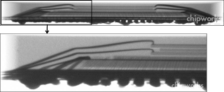
Someone did a comparison of the size of the heat spreader cap on the XBSS and it came out to ~190 mm, much smaller than XBSX heat spreader so it has it's own dedicated SoC, it's not just binned XBSX production
Last edited:
So I was thinking about the cooling patent and the fact that we could see 2 stacked chips (5c and 5d) inside the main chip (this is a modified version of it):

What's interesting is that Cerny already designed a very innovative chip-on-chip design for Vita with the memory stacked on top of the APU.
https://www.semiconductor-digest.com/2012/07/06/sonys-ps-vita-uses-chip-on-chip-sip-3d-but-not-3d/
So as they already have experience doing so, I won't be surprised if they do something similar on PS5, even if it's not done on the main APU. Now what part of PS5 could use the patent design? Well, the I/O complex is comprised of several chips (that could be stacked to save space) and it'll probably need active cooling so it could be a good candidate for that design. The flash controller could also be a good candidate (the I/O complex seems to be part of the main APU?).
anexanhume
Veteran
It's not clear to me, at least with the current technical disclosures, why they would need this for the PS5. I'm still eagerly anticipating the teardown for the custom liquid metal barrier alone.So I was thinking about the cooling patent and the fact that we could see 2 stacked chips (5c and 5d) inside the main chip (this is a modified version of it):
What's interesting is that Cerny already designed a very innovative chip-on-chip design for Vita with the memory stacked on top of the APU.
https://www.semiconductor-digest.com/2012/07/06/sonys-ps-vita-uses-chip-on-chip-sip-3d-but-not-3d/
So as they already have experience doing so, I won't be surprised if they do something similar on PS5, even if it's not done on the main APU. Now what part of PS5 could use the patent design? Well, the I/O complex is comprised of several chips (that could be stacked to save space) and it'll probably need active cooling so it could be a good candidate for that design. The flash controller could also be a good candidate (the I/O complex seems to be part of the main APU?).
- Status
- Not open for further replies.
Similar threads
- Replies
- 96
- Views
- 8K
- Locked
- Replies
- 3K
- Views
- 241K
- Replies
- 22
- Views
- 7K
- Replies
- 3K
- Views
- 273K
- Locked
- Replies
- 27
- Views
- 2K