anexanhume
Veteran
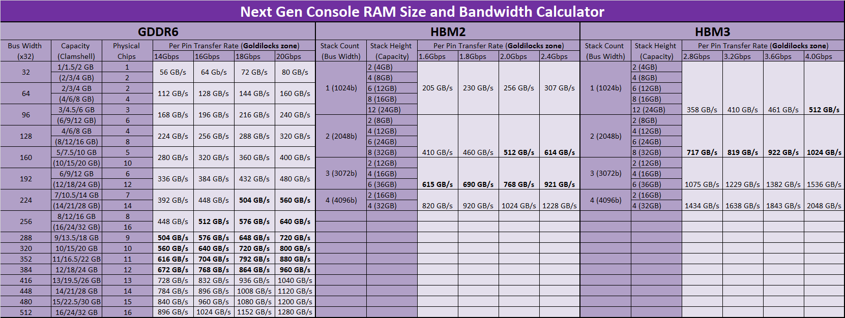
How is 528 GB/s obviously 256-bit but 560 GB/s is obviously 320-bit?On contrary, it pretty much points to 320bit bus. Theoretical for both Arden and Ariel seem to be using 14Gbps RAM modules, therefore 560GB/s would point at 320bit bus with 14Gbps RAM modules.
View attachment 3623
As we have seen with Oberon, theoretical value for BW does not mean you cannot go higher if there are higher clocked RAM chips out there (which Flute and Oberon tests both confirm).
Also, nice to see my memory chart is being used by others

Here's the whole thing: