Next Generation Hardware Speculation with a Technical Spin [post E3 2019, pre GDC 2020] [XBSX, PS5]

Status
Not open for further replies.
Can someone do the math on extrapolating the newly announced AMD 4000 series APU's to larger CU counts?
Surely taking the 4800U (15W) and 4800H (45W) both with 8CU's and isolating the CPU size from the CU size cen help us make a guesstimate of the total size of a 36CU, and 56CU APU would look like?
Anandtech seems to think approx 148mm2 for the total APU area. whats the latest info on a RDNA CU unit in size?
As these are the first Zen chips with only 8Mb L3, the CPU is a bit more of a guess too...

Anyway, it's another data point for us to use in discussion.
Once people start benching these APU's it will be a much more powerful indicator of size/power usage/ and total perf. of the next consoles...
 
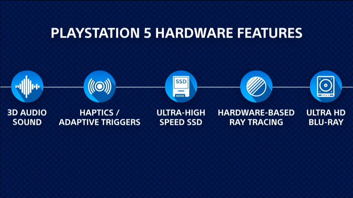
New Logo and features recap.
ENpAXw5UwAAKCV-.jpg

ENpAekxUcAA3vf8.jpg

I think the SSD will not respect the NVMe norm and will not use PCIE bus. They will probably use a direct connection to HBCC controller like in The Radeon Pro SSG.

It will help with cost with less complexity inside the controller because they will not need to respect NVMe norm and every unuseful features for a console and it will help with performance no need to go through the PCIE bus.

Does the HBCC allow the CPU to access the memory hanging off the GPU via the HBCC?
I'm not sully informed of how system RAM is managed in modern consoles with a single shared memory space,
but i would be surprised if it still isn't owned and primarily managed by the CPU, rather than the GPU.

I think that having the CPU be able to access 100+ Gbs of data @ NVME speeds would enable a lot of new functionality in world building and game design.
IF the NVMe/SSD is only an extension of the GPU memory, then it ends up being much less useful... imho...
 
I think the SSD will not respect the NVMe norm and will not use PCIE bus. They will probably use a direct connection to HBCC controller like in The Radeon Pro SSG.

It will help with cost with less complexity inside the controller because they will not need to respect NVMe norm and every unuseful features for a console and it will help with performance no need to go through the PCIE bus.

?

The SDDs on the Pro are connected to the GPU using a PCIE bus and bridge chip. The onboard SDDs are suppose to sit between the local VRAM and system RAM. But on consoles VRAM and system RAM are part of the same unified pool of GDDR.
 
Alright broke out the measurement taping and found out some things about Navi and the Anaconda in terms of sizes on 7nm.
5700:
GDDR6 phy controller: 4.5mm x 8
Dual CU: 3.37mm x 20
4 ROP cluster: .55mm x 16
L1+L2+ACE+Gemotry processor+empty buffer spaces + etc: 139mm

Now Anaconda:

A rougher estimate using the 12x14mm GDDR6 chips next to the SOC.

370mm-390mm.

It's a bit bigger than the 1X SOC for sure.

If we use the figure of 380mm,

75mm for CPU
45mm for 10 GDDR6 controllers
8.8mm for ROPs
140mm for buses, caches, ACE, geometry processors, shape etc. I might be over estimating this part as the 5700 seems to have lots of "empty" areas.

We have ~110mm left for CUs + RT hardware. There is enough there for ~30 dual CUs and RT extensions.

Conclusion:

The Anaconda SOC is around the minimum size you need to fit the maximum Navi GPU and Zen2 cores.

I expect Anaconda to have a minimum of 48 CUs if the secret sauce is extra heavy or 60CUs if the sauce is light.

I did a calculation of the Scarlett die vs Scorpio die using the new picture, it's 10.625% larger. 397mm2.

Surprising enough I got this figure on my first pass at the E3 teaser! I later revised it down to 360-370mm2 using what ever rounding error i can because I refused to believe that the Xsx chip was this much of a monster.
 
?

The SDDs on the Pro are connected to the GPU using a PCIE bus and bridge chip. The onboard SDDs are suppose to sit between the local VRAM and system RAM. But on consoles VRAM and system RAM are part of the same unified pool of GDDR.

I was not knowing I was thinking it has another bus, it will be different but I think the PS5 SSD will not use PCIe. And they never said NVMe, it will not respect the norm for cost probably.
 
I did a calculation of the Scarlett die vs Scorpio die using the new picture, it's 10.625% larger. 397mm2.

Surprising enough I got this figure on my first pass at the E3 teaser! I later revised it down to 360-370mm2 using what ever rounding error i can because I refused to believe that the Xsx chip was this much of a monster.


Still enough for 56 active / 60 on-die CUs ?
 
Can someone do the math on extrapolating the newly announced AMD 4000 series APU's to larger CU counts?
Surely taking the 4800U (15W) and 4800H (45W) both with 8CU's and isolating the CPU size from the CU size cen help us make a guesstimate of the total size of a 36CU, and 56CU APU would look like?
Well, we will first need to know what's the size of the newly redesigned Vega hardware inside those APUs. Lisa has said that they have redesigned more than 50% of that Vega part to be more power efficient.
 
So the RX 5600XT with it's 36CU and 1375MHz clock, has a TDP of 150w, compared to 225w for the 5700XT with it's 40CU, 1775MHz clock, which is a 50% increase in power for a 10% increase in CU count + 30% clock uplift, which clearly means all those theories about going wider at low clocks will not mean much regarding power consumption, You'd have to go way down on clocks for that factor to take effect.

With that in mind, I expect a 56CU part clocked at 1.7GHz to consume no less than 300w, maybe with some voltage selection you can bring that down to 280w, and that is a BIG maybe, as it will still be silicon lottery.
 
Status
Not open for further replies.
Back
Top