Silent_Buddha
Legend
I can see the headlines now:
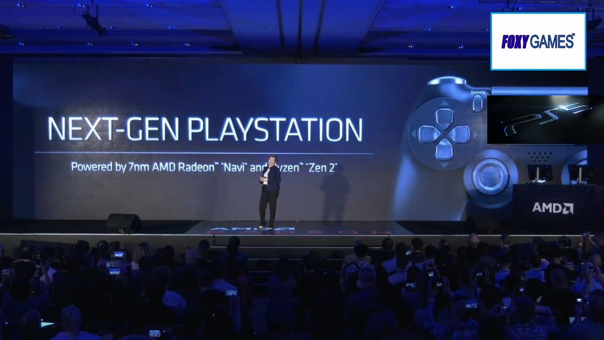
You're not seeing the big picture. That's actually a photograph of the retail PS5.

Regards,
SB
I can see the headlines now:
Ok, that's a specific point. But you have to agree it's nothing in practice because it's mostly avoidable to use trig (i don't use it a single time, although i have cones, discs, and intersections with those).RDNA can do more SINE ops per second than GCN
Complexity is irrelevant for the TF measure. I can't help it.Short answer is, processors are too complex to be described with a number, but human beings can't help themselves and will keep talking about flops.
It's not nitpicking but making important clarifications with regards the exactness of what you stated. You posted a pure, logical assertion, "1==1, period." Anyone looking up how GPUs work could think that's how it works, but it isn't. Now if you are saying that in real terms, it makes no difference because of the flops actually being used RDNA will see no advantage, you have an argument, but that's different to saying "1==1" and it's also along the lines of people saying 1 GCN TF != 1 RDNA TF because in real world terms, utilisation is better where you called it bullshit.So, nice try, but - damn, you could just adimt 1TF==1TF and call it a day. Now we end up in nit-picking.
Obviously he's not expecting robots to be consumer products so could it be stealth Horizon Zero Dawn II hype? If Sony do show a real time trailer of it, hopefully it's on par with Hellblade II graphics wise which should give more hope of a 13 TF PS5. If it's Godfall level then cancel Project PS5 altogether!

 What to make of it? Certainly, whatever Sony did, secrecy was not kept at highest level. Throughout the year we could see a chip, most certainly from Sony, going through revisions and updates, perhaps earlier then expected considering console is scheduled for next year.
 Between Liverpool, Neo and Scorpio, you can see the drop in bandwidth per flop already; the larger L2 size and colour/ROP compression help mitigate it in certain scenarios, but that's clearly not a magical fix to the larger issue.It will definitely be the bottleneck it next gen. Looking at 320 GB/s on X1X but only 512 for XSX is clearly just not enough for double the TF power.
Is this trying to suggest Nintendo is making a new console with a chip from AMD? I have a hard time believing this with the success of the Switch, it's way too soon for a replacement in that regard imo.
Sparkman seems to be Lockhart according to recent leaks.Is this trying to suggest Nintendo is making a new console with a chip from AMD? I have a hard time believing this with the success of the Switch, it's way too soon for a replacement in that regard imo.
Also shouldn't there be 2 chips for the 2 xbox consoles that are expected. Nobody seems to be looking into Lockhart it seems.
So with all info we have now, I will try to paint current picture we have regarding hypothetical PS5.
*note that alot of info below is alleged and obviously not confirmed
PS5
- 1st Initial info January (Gonzalo 1.0)
- First info regarding what is likely PS5 codename came in January, when Gonzalo chip leaked by Komachi/APISAK
- Actual codename string heavily indicated semi custom game console chip (2G)
- Gonzalo codename 2G16002CE8JA2_32/10/10_13E9 contained iGPU part from Ariel
- 8 core Zen2 3.2GHz
- Navi10 at 1.0GHz
- Ariel could be found in PCI device repository https://pci-ids.ucw.cz/read/PC/1002/13e9 with iGPU also surfacing in January- 13e9
- 2nd leaked info April (Gonzalo 2.0)
- Reported by APISAK -
- Gonzalo codename ZG16702AE8JB2_32/10/18_13F8 containing iGPU associated with Ariel
- 8 core Zen2 3.2GHz
- Navi10 at 1.8GHz
- 3rd PS5 devkit PCB specs from OQA leaked in May
- Posted on May 21st by now deleted redditor
- Containing very specific alleged motherboard details
- 316mm2 SOC
- 32GB of RAM
- 256bit bus - 18Gbps memory from Samsung ~ 576GB/s (important part, as it correlates with 2 other following rumors)
- 4GB of DDR4
- 2TB of SSD with soldered DRAM
- 4th leak Gonzalo 1.8GHz FS score of 20k+ in June
- APISAK leaked Gonzalo FS score (scored 2x compared to ES2 version - 1GHz)
- 5th Flute benchmark leaked by Komachi in June
- Flute benchmark was leaked in June showing a custom AMD chip score on Userbenchmark deleted following date
- Contained following
- 13F9 iGPU (likely revision matching Gonzalo iGPU)
- 8 core Zen 2 clocked at 3.2GHz and with what looks to be 8MB of L3 cache (1/4 of desktop variant)
- 16GB of RAM on 256bit bus and ~530GB/s of bandwidth
- This part is very important as it corelates with 2 rumors (PCB leak from May and AMD github leak from December)
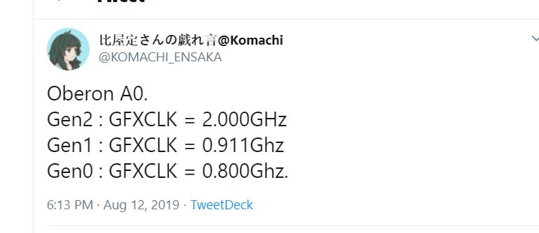
- 6th Oberon leaked by Komachi in August
- Oberon was chip with matching clocks for both PS4 and Pro consoles
- Now, after AMD Github leak, we see Oberon is Ariel revision (perhaps final chip vs dev kit one?)
- Oberon appears to be exact match for Ariel, therefore Gonzalo/Flute
- 7th Taiwanese forum rumor
- Linked by Komachi back in October when Sparkman (Lockhart?) appeared
- Seems to contain info on chips currently passing verification and fab process
- Contains Oberon/Arden(XSX) info with Arden being "one size" larger then Oberon (~50mm2)
- 8th AMD GIthub repo leak December
- Very important leak as it provided incredible insight in what appears to be next gen AMD products
- Aside from one (Navi10), no other mentioned GPU has been released yet
- Contains Ariel/Oberon regression tests
- Was created on May 2018 and updated through 2019 to July
- Oberon latest revision appears to be May
- What it provides is following
- Ariel - Oberon link. Both appear to be same chips, just Oberon being later revision
- GPU specification - 36CUs with 64ROPs clocked at 2.0GHz at in native mode - 9.2TF
- 256bit bus with memory BW evolution from 448GB/S to 530GB/s in Oberon B0 (Flute and PCB leak??)
- Indicating usage of 14Gbps chips to 18Gbps one later with Oberon
- 800MHz and 911MHz, along with downclocked BW matching PS4 and PRO BC
Huh...was long
BUT, given that we know devs have had PS5 "V" dev kits since summer, it is to assume with certainty that actual APU has been developed and sent to developers at that time, and dev kits used at that point were not ones containing PC parts.
From this, we can say that Ariel/Oberon was most certainly PS5 chip. Is it still one unchanged? I think so, would be extremely hard to think chip smaller then XSX one and still going through verification and fab process to be old chip not meant to be used.
So, specs...All points to following :
8 core Zen 2 CPU clocked at 3.2GHz with 1/4 of L3 cache
9.2TF Navi GPU with RT and VRS
36CU clocked at 2.GHZ / 64ROPs / 288GT/s of texture fillrate / 128GP/s of pixel fillrate
16GB GDDR6 on 256bit bus / 576GB/s
1TB of custom made SSD
Can this be delivered at 399$ and has Sony botched design of next gen console? I believe answer to both is no.
This console is almost certainly pushing boundaries of classic console design (even with design and N7P node improvements this is ~200W at least), and with RT hardwared + custom SSD it is certainly not gonna come cheap. For customer or Sony, someone will pay the difference.
IMO its hard to believe Sony aimed at something higher then XSX, as that console is specifically made as premium SKU with form to match. If Sony aimed at best possible console for relatively acceptable price and TDP, then console above cannot be called conservative. This one is pushing things more then either PS4 or Pro have.
In comparison with what we know and assume of Arden, I would say difference between the two is AT MOST half that of Xbox One X vs Pro, therefore could be considered very close. In fact, if we are to go and look for similar gap to consoles, we would probably have to go back to PS360 era.
I remain skeptical of that 2GHz clock. Thermal density is going to be very challenging, they cannot really bin the chips for a console. Is Navi that good? 7nm+?
Its from Taiwanese forum. I think this is someone who has info on production line in TSMC and has no idea about Lockhart thing...He assumes Sparkman is too small for next gen I believe.Is this trying to suggest Nintendo is making a new console with a chip from AMD? I have a hard time believing this with the success of the Switch, it's way too soon for a replacement in that regard imo.
Also shouldn't there be 2 chips for the 2 xbox consoles that are expected. Nobody seems to be looking into Lockhart it seems.
Its from Taiwanese forum. I think this is someone who has info on production line in TSMC and has no idea about Lockhart thing...He assumes Sparkman is too small for next gen I believe.
The 2GHz clock is pretty much impossible to explain. Everything that is known suggests it's unrealistic.I remain skeptical of that 2GHz clock. Thermal density is going to be very challenging, they cannot really bin the chips for a console. Is Navi that good? 7nm+?

Of course, but its up to us to kinda suspect who has right info and what to make of it. Ever since I remember next gen info came unexpexted and from weird sources (360 diagram in 04', Durango and Orbis, PCB/Komachi etc.)He has info but his speculations are beyond awful.
He thinks the 50mm2 difference between Arden and Oberon is because of RT, and because of 56 vs 36 CUs.
I don't think it's too unrealistic, 7nm+ should bring some clock headroom, it only needs a ~10% clock increase from the 5700xt, not too far out of the picture. A bit optimistic but not impossible. 7nm has shown to be able to hit >2ghz, just at very high power draw, maybe 7nm+ will help with it.The 2GHz clock is pretty much impossible to explain. Everything that is known suggests it's unrealistic.
Of course, but its up to us to kinda suspect who has right info and what to make of it. Ever since I remember next gen info came unexpexted and from weird sources (360 diagram in 04', Durango and Orbis, PCB/Komachi etc.)
Alot of times these people dont even care about console stuff.
I don't think it's too unrealistic, 7nm+ should bring some clock headroom, it only needs a ~10% clock increase from the 5700xt, not too far out of the picture. A bit optimistic but not impossible. 7nm has shown to be able to hit >2ghz, just at very high power draw, maybe 7nm+ will help with it.