
This might be related to the works on a custom accelerator for the Frontier super computer. It should be ready in 2021 for DoE & Oak Ridge labs.I noted the first time around that this comes from a Department of Energy research program into HPC, which going by the history of other such patents from DOE programs has either a low chance of being used or a long timeline for being seen. Some of the low-voltage and variable-SIMD patents that people were clamoring about in 2016 (filed in 2014) as possibly being Vega or Navi-related have not shown up for either three years later, so if the trend persists it won't be applicable to any chip currently in the rumors for the near or mid-term.
You are using an out of date browser. It may not display this or other websites correctly.
You should upgrade or use an alternative browser.
You should upgrade or use an alternative browser.
AMD: Navi Speculation, Rumours and Discussion [2019-2020]
- Thread starter Kaotik
- Start date
- Status
- Not open for further replies.
Betonmischer
Newcomer
After playing around with the updated Radeon GPU Profiler, which introduced Navi support, I discovered that not only NGG pipeline is now active for triangle culling via Primitive Shaders, but Surface Shaders seem to be working as well. I've captured a frame trace from Shadow of the Tomb Raider featuring some tessellation. Compared to the same frame from Vega, NGG Surface Shaders have now completely replaced the Hull Shader stage.
Attachments

Frenetic Pony
Veteran
This might be related to the works on a custom accelerator for the Frontier super computer. It should be ready in 2021 for DoE & Oak Ridge labs.
Isn't this just likely to use Arcturus? Never got the impression the "fastest computer" race cared at all about power efficiency, not when data bandwidth and latency are the major obstacles to scalability. If the resulting center needs it's own solar + battery installation just for power along with being built next to a water source just for cooling then so be it.
The Exascale initiative started a goal of exaflop-scale performance within a power footprint of 20 MW. While this is massive in consumer terms, it is constricted considering the number of nodes (thousands or tens of thousands) that have to share it along with the infrastructure supporting them.
There seems to have been some admission with the latest roadmaps that this efficiency isn't going to happen on-time. The latest aspirations are for up to 40 MW (possibly pushed to 60), although some stories indicate some were hoping to stay near or below the original 20 MW.
While it may be possible to scale to an even higher facility power cost, there is a desire to limit the operational costs and the scale of the electrical delivery and power dissipation out of a single facility.
anexanhume
Veteran
I’m reminded of this:After playing around with the updated Radeon GPU Profiler, which introduced Navi support, I discovered that not only NGG pipeline is now active for triangle culling via Primitive Shaders, but Surface Shaders seem to be working as well. I've captured a frame trace from Shadow of the Tomb Raider featuring some tessellation. Compared to the same frame from Vega, NGG Surface Shaders have now completely replaced the Hull Shader stage.
The two-layer structure of task and mesh shaders is broadly similar to that of tessellation hull and domain shaders. While it doesn’t appear that mesh shaders have any kind of access to the fixed-function tessellator unit, it’s also not too hard to imagine that we could write code in task/mesh shaders to reproduce tessellation functionality (or at least some of it). Figuring out the details would be a bit of a research project for sure—maybe someone has already worked on this?—and perf would be a question mark. However, we’d get the benefit of being able to change how tessellation works, instead of being stuck with whatever Microsoft decided on in the late 2000s.
From here: http://www.reedbeta.com/blog/mesh-shader-possibilities/
Navi 14
4.4.14694 Compatibility Profile Context FireGL 19.40 26.20.197.4527
VS Radeon Pro WX 7100 (Polaris, 36CU)
Only tesselation result
Tessellation
4.4.14694 Compatibility Profile Context FireGL 19.40 26.20.197.4527
VS Radeon Pro WX 7100 (Polaris, 36CU)
Only tesselation result
Tessellation
- Onscreen 18488 Frames (616.3 Fps) Navi 14
- Offscreen 53930 Frames (898.8 Fps)
- Onscreen 10539 Frames (351.3 Fps) WX 7100
- Offscreen 47312 Frames (788.5 Fps)
D
Deleted member 13524
Guest
There are off-screen results too, which AFAIK forces the same 1080p resolution regardless of the panel connected.Only on-screen tesselation result
D
Deleted member 90741
Guest
Navi12 Support is in the staging pipeline for Linux
https://lists.freedesktop.org/archives/amd-gfx/2019-August/037821.html
Not much info except that it uses the same code path like the rest of the NV Family
From LLVM I see that Navi12 does not have the FeatureLdsMisalignedBug, what is this issue?
https://lists.freedesktop.org/archives/amd-gfx/2019-August/037821.html
Not much info except that it uses the same code path like the rest of the NV Family
From LLVM I see that Navi12 does not have the FeatureLdsMisalignedBug, what is this issue?
There's a comment concerning this bug occurring when workgroup processing is enabled. Other than that, I haven't seen additional details.Navi12 Support is in the staging pipeline for Linux
https://lists.freedesktop.org/archives/amd-gfx/2019-August/037821.html
Not much info except that it uses the same code path like the rest of the NV Family
From LLVM I see that Navi12 does not have the FeatureLdsMisalignedBug, what is this issue?
https://gpuopen.com/wp-content/uploads/2019/08/RDNA_Shader_ISA_7July2019.pdf
RDNA 1.0 Instruction Set Architecture Reference Guide, 240 pages
RDNA 1.0 Instruction Set Architecture Reference Guide, 240 pages
DmitryKo
Veteran
It used to be far easier to reverse-engineer the silicon with semiconduction production processes of the past; here is the ARM1 die from 1985, produced at 1 µm. Today's 7 nm should be like 150 times smaller, even the best die shots by Fritzchens Fritz are unable to resolve such fine details.I think the LDS is past the first set of SIMD blocks and before the front end because there's SRAM roughly in the shape and capacity as a register file, but not part of the SIMD blocks.
OK, I'm oficially baffled as to why only 10-20% of the die surface is seemingly used for the actual logic, and why a thick copper layer covers the entire remaining surface (it has to be sanded off to reveal the die).There's only one layer of active transistors, with the rest being interconnect and elements like power planes and inductors/capacitors.
I believe we are looking at the back of the wafer substrate which actually faces down in the production process.
The actual gates (transistors) are develped on the top (i.e. on the opposite side), then attached to multiple local and global copper interconnect layers interspersed with dielectric layers, and finally solder balls are attached to the interconnects
Then the wafer is turned upside down and cut to slices and each chip's solder balls are connected to a curcuit board .
If so, why these sparsely placed blocks of silicon are even visible, and why the usable die area is so small with the rest being just copper layer?
I thought it could be some fancy multi-layer 2.5D package where SRAM is attached with TSVs to the actual logic below and the substrate wafer seves as an interposer for the SRAM layer - but then those fixed-function 0.18 micron videochips from 2000s look pertty much the same:
Their numbering of cache levels is a bit incoherent (pun intended).
In paragraph 2.3. Data Sharing the hierarchy is presented as L0 (Texture R/W Cache), L1 (Graphics L1 - this is new for RNDA), and L2 (Read/Write Cache per Memory Channel).
And then in Programming Model Changes they say "... DLC bit (Device Level Coherence) to control level-1 caching" and in paragraph 8.1.10. GLC, DLC and SLC Bits Explained
they say "The Device Level Coherent bit (DLC) and System Level Coherent (SLC) bits control the behavior of the second and third level caches".
LDS is actually 128 KB per WGP, though shared by the two CUs....I would say that LDS should be 4 times as big in total size as it was in GCN CU - i.e. 128 KB per each CU (with 2 SIMD32 vector units) and 256 KB per WGP (2 CUs and 4 SIMD32 vector units).
https://gpuopen.com/wp-content/uploads/2019/08/RDNA_Shader_ISA_7July2019.pdf
RDNA 1.0 Instruction Set Architecture Reference Guide, 240 pages
I skimmed the document and figured I could comment on some of the elements that stood out to me, and on some things that matched up with what has been discussed here.
Wave32 and Wave64 mode were described in more detail, with some additional features described. GCN has historically not skipped instructions if their EXEC masks were all 0. Wave64 instruction streams are composed of two Wave32 instructions, and for VALU instructions one or both halves can be skipped if they don't write to a scalar register or condition code. Vector memory can skip one half of the execution, but not both.
There's an LLVM bug flag mentioned in this thread for when texture and vector memory instruction failure if the EXEC mask is 0 for the low or high half, perhaps related to that last point?
Since Wave64 is implemented as two Wave32 instructions, there are certain corner cases where the code must take care avoid unpredictable behavior, like if the two instructions write to a common destination like a scalar register that the other half interacts with.
The AMD slides showed Wave64 as taking a 64-wide wavefront instruction and splitting it into two adjacent Wave32 instructions, but the ISA doc mentions a subvector execution mode, where instead of executing the paired instructions sequentially, a loop is constructed with a pair of special instructions that executes half of the wavefront all the way through, then repeats the loop for the other half. This may improve performance by fitting better in the cache and allowing for a special case of register allocation--wave-temporary registers. This may evoke memories of some things like clause-temporary registers back in the VLIW days (more on clauses later), and takes advantage of the split execution loop to save having to allocate a portion of the wavefront's register space for both halves of the loop. Special care is needed if the running part of the loop may zero-out its half of the execution mask, since that confuses how the CU keeps track of where it is in the process.
The LDS physically has a layout similar to there being 2 GCN LDS arrays next to each other. Each LDS half is local to nearest SIMDs, though in workgroup processing mode they can access data in the other half, with potential unspecified performance penalties. There is an LLVM bug flag discussing some sort of problem with wider misaligned LDS accesses in this mode, perhaps related to some sort of issue dealing with LDS accesses that somehow straddle the two halves while taking variable numbers of cycles in each to complete.
As noted in other changes, SGPRs are no longer parceled out between wavefronts, each wavefront gets a fixed amount.
The DLC bit seen in some LLVM commits is confirmed to deal with caching in the L1. The L1 seems to be more for amplifying read bandwidth, as writes still list the L2 as their destination.
The earlier mention of a separate counter for vector loads and vector stores is confirmed.
Vector instructions may usually be able to source two scalar registers instead of one with GCN--this has come up as something of a bottleneck in some developer presentations.
Some instructions that recognized SIMD width did need to change, like some of the DPP and permute options.
A number of instructions have been dropped entirely, including the branch stack management with FORK and JOIN and VSKIP, which were hinted at earlier.
This thread mentioned an instruction a few times called S_INST_PREFETCH, which has code mentioning it in LLVM and a bug flag. The instruction itself is not currently in the ISA doc, although certain elements surrounding it like a mention of a 4-cache line stride seem to mirror a section on shader instruction padding--where aggressive prefetching makes it necessary to pad out 256 bytes at the end of a shader in case it prefetches into forbidden locations.
There are mentions of primitive shader export instructions.
Another miscellaneous item is that there's a new use for scalar register ID 125, which serves as a permanent zero when read and ignores any writes to it. I mention this in the context of GCN being described at times as being more RISC-like, as this is something RISC ISAs have done before, although in this context it is surrounded by very complex behavior and is partially redundant with scalar ID 128 (hard-wired zero for reads). I suppose this happens when the decision to expose this waits 6+ generations, although 125 has been reserved since Southern Islands.
The LLVM changes have a flag indicating there are no software-defined wait states, and section 4.5 which has always had a growing table of such hazards is empty for RDNA.
An earlier note of the non-sequential addressing instruction format for imaging instructions has been confirmed to mean that there are texturing instructions that no longer require that all their address registers be in sequential registers, at the cost of having a variable number of 32-bit sections to the instruction encoding (up to 5 dword in total worst-case).
To finish a thought I started earlier about clauses, RDNA introduces an instruction that defines a mode where long streams of certain instruction types can monopolize the wavefront scheduling for that type. The CU will no longer let another wavefront issue instructions of that type until the current wavefront reaches some kind of exit condition.
The instruction, S_CLAUSE, will let a wavefront get exclusive instruction issue in subsequent cycles for whatever type of instruction comes immediately afterward (if of the following types: VALU, SMEM, LDS, FLAT, Texture, buffer, global and scratch). Most of these are some kind of memory access, outside of VALU. The clause continues until an instruction of a different type is encountered, at which point it automatically ends. There may be a number of other exit conditions, as there seems to be a mention of a numerical limit for scalar memory.
One possible source of confusion here is that AMD has used the word clause in different ways. VLIW GPUs had clause types similar to this, with ALU clauses and a variety of memory-access type clauses. The details of what makes up those memory types has changed. For example, the LDS type has been promoted to be its own clause, and vertex fetch isn't its own type.
VLIW clause instructions are heavier in weight, have explicit types instead of checking what the next instruction type is, and have explicit counts for how many instructions they contain instead of automatically detecting when a new instruction type is fetched.
The monopolization of instruction issue is somewhat akin to VLIW, although the wording in the RDNA doc seems less clear on whether it's monopolizing all instruction issue or just the issue of the specific type within a CU.
For GCN GPUs, the clause term showed up on occasion, but this seemed to be more of a description of when many instructions of the same type occurred in a row rather than a hard-defined clause. For RDNA, these seem to have been been renamed as instruction groups, while the term clause has been promoted to a run of the same type of instructions whose issue is architecturally-enforced with S_CLAUSE.
What penalties and benefits there are aren't wholly spelled out. VLIW had large ~40 cycle penalties for changing clauses, but RDNA's GCN heritage would give a much lower overhead due to it switching wavefronts more often. Whether that means zero switching overhead isn't clear, I think there is some loss if switching happens too often.
On the other hand, a clause monopolizing instruction issue would presumably hurt CU throughput, although it may allow for faster run-through of phases of execution like setup or writeback that might benefit from not having interference from other wavefronts.
(edit: Clauses also showed up with ARM's GPU architecture for arranging execution (not type based?). They were ISA elements in Bifrost that were then dumped with Valhall.)
The now-top of the die has some layer of silicon substrate, which could be thinned if desired or left for mechanical stiffness. I'm not sure if Polaris had something plated onto it or deposited. Zen did have an alloy plated onto that part of the die to allow for soldering to the heat-spreader.
The description is that it's sanding through the IHS, if that's what is on top of the die.
The instruction, S_CLAUSE, will let a wavefront get exclusive instruction issue in subsequent cycles for whatever type of instruction comes immediately afterward (if of the following types: VALU, SMEM, LDS, FLAT, Texture, buffer, global and scratch). Most of these are some kind of memory access, outside of VALU. The clause continues until an instruction of a different type is encountered, at which point it automatically ends. There may be a number of other exit conditions, as there seems to be a mention of a numerical limit for scalar memory.
One possible source of confusion here is that AMD has used the word clause in different ways. VLIW GPUs had clause types similar to this, with ALU clauses and a variety of memory-access type clauses. The details of what makes up those memory types has changed. For example, the LDS type has been promoted to be its own clause, and vertex fetch isn't its own type.
VLIW clause instructions are heavier in weight, have explicit types instead of checking what the next instruction type is, and have explicit counts for how many instructions they contain instead of automatically detecting when a new instruction type is fetched.
The monopolization of instruction issue is somewhat akin to VLIW, although the wording in the RDNA doc seems less clear on whether it's monopolizing all instruction issue or just the issue of the specific type within a CU.
For GCN GPUs, the clause term showed up on occasion, but this seemed to be more of a description of when many instructions of the same type occurred in a row rather than a hard-defined clause. For RDNA, these seem to have been been renamed as instruction groups, while the term clause has been promoted to a run of the same type of instructions whose issue is architecturally-enforced with S_CLAUSE.
What penalties and benefits there are aren't wholly spelled out. VLIW had large ~40 cycle penalties for changing clauses, but RDNA's GCN heritage would give a much lower overhead due to it switching wavefronts more often. Whether that means zero switching overhead isn't clear, I think there is some loss if switching happens too often.
On the other hand, a clause monopolizing instruction issue would presumably hurt CU throughput, although it may allow for faster run-through of phases of execution like setup or writeback that might benefit from not having interference from other wavefronts.
(edit: Clauses also showed up with ARM's GPU architecture for arranging execution (not type based?). They were ISA elements in Bifrost that were then dumped with Valhall.)
I'm pretty sure it's some kind of flip-chip integration, so the upper surface should be the closest to the transistor layer. What's above it is the silicon substrate, which should be uninvolved with internal interconnects. All of the metal layers would be below that surface (hence flip-chip), and I assume what is being scraped off isn't those layers since I didn't see any solder balls or other elements on the surface.It used to be far easier to reverse-engineer the silicon with semiconduction production processes of the past; here is the ARM1 die from 1985, produced at 1 µm. Today's 7 nm should be like 150 times smaller, even the best die shots by Fritzchens Fritz are unable to resolve such fine details.
OK, I'm oficially baffled as to why only 10-20% of the die surface is seemingly used for the actual logic, and why a thick copper layer covers the entire remaining surface (it has to be sanded off to reveal the die).
The now-top of the die has some layer of silicon substrate, which could be thinned if desired or left for mechanical stiffness. I'm not sure if Polaris had something plated onto it or deposited. Zen did have an alloy plated onto that part of the die to allow for soldering to the heat-spreader.
The description is that it's sanding through the IHS, if that's what is on top of the die.
If the blocks you mean are those on the perimeter, those would mostly be PHY and analog devices. Those are physically larger since they operate at different and frequently higher voltages, and analog properties are more closely aligned with physical dimensions. I think their implementation can lead to them etching much deeper into the silicon, and so in the reverse situation scraping from below would reach elements of them sooner.If so, why these sparsely placed blocks of silicon are even visible, and why the usable die area is so small with the rest being just copper layer?
Perhaps that's a wire-bonded chip rather than flip chip? An earlier picture showing the plastic enclosure being broken seemed to show wire bonding, and in that case we wouldn't have the flipped order of transistor and metal layers of modern chipos. Then, the PHY and non-transistor layers would be sanded through first.I thought it could be some fancy multi-layer 2.5D package where SRAM is attached with TSVs to the actual logic below and the substrate wafer seves as an interposer for the SRAM layer - but then those fixed-function 0.18 micron videochips from 2000s look pertty much the same:
Last edited:
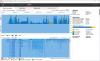
@CarstenS I read your article good written, but there are no values of the beyond3d Suite date.  Maybe next time you can write some numbers in a Table?
https://www.heise.de/select/ct/2019/17/1565695001742590
Maybe next time you can write some numbers in a Table? https://www.heise.de/select/ct/2019/17/1565695001742590
Sorry, but there was no space left for a large table (and a small table would not have done the suite justice). I will put something up on my website later this week, have an 5700XT now myself, so I can do benchmarks completely independent from work.
itsmydamnation
Veteran
Make you to link it here when your doneSorry, but there was no space left for a large table (and a small table would not have done the suite justice). I will put something up on my website later this week, have an 5700XT now myself, so I can do benchmarks completely independent from work.
- Status
- Not open for further replies.