
Bondrewd
Veteran
None of what they said is a GCN problem.Doesn't sound like a GCN problem to me.
All either their legacy from days before it or just plain lower quality circuit design.
None of what they said is a GCN problem.Doesn't sound like a GCN problem to me.
Guys, before you argue endlessly about whether GCN is the problem, you should start by defining what you mean by "GCN". The debate makes no sense whatsoever otherwise.
Doesn't sound like a GCN problem to me.

Komachi in general has been trustworthy leaker for what I can remember, but didn't he quickly delete the tweet where he said 8x5CU?`Which could indicate it wasn't solidSo I guess everyone has decided that the rumor/leak from KOMACHI that Navi has 8 shader engines is false then? And everyone must have also decided therefore that Navi is using more than 40 compute units to compete with the 2070? Because I'm not sure how a GCN based GPU is supposed to beat a 2070 with 40 CUs at a vaguely sensible TDP without some sort of architectural advancement to GCN?
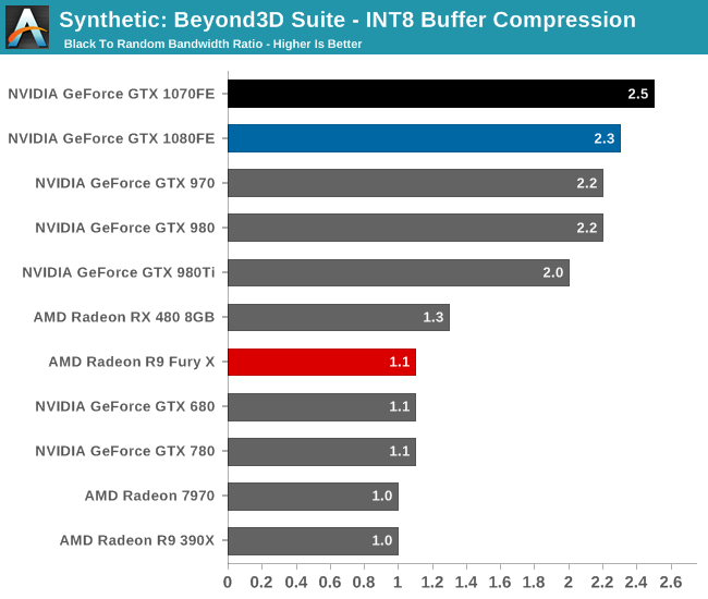
Did Beyond3D ever provide the source code for these tests? I'm reasonably sure they were at least partly debunked.Maybe not, but the question still remains ... but why since R9 AMD failed to equate Nvidia's efficiency and still needs a lot more bandwith? (I know Vega 56/64 uses bining, looked deferred like Nvidia ...)
I think this rumour could have merit. Though it might be for the wrong GPU?So I guess everyone has decided that the rumor/leak from KOMACHI that Navi has 8 shader engines is false then? And everyone must have also decided therefore that Navi is using more than 40 compute units to compete with the 2070? Because I'm not sure how a GCN based GPU is supposed to beat a 2070 with 40 CUs at a vaguely sensible TDP without some sort of architectural advancement to GCN?
The Zen vs BD comparison becomes a question of architecture versus microarchitecture. The x86 architecture defines instructions and a range of behaviors to software, and the Zen, BD, or Skylake architectures are implementations of said behaviors. The particulars of what they use to carry out their architectural requirements and how well or not well they handle them are things the architecture tries to be somewhat agnostic about. That being said, implementation quirks throughout history can be discerned if one know the context of things like x87, FMA3, the often winding encoding and prefix handling, etc.Oh boy. When you keep the scope of changes done between BD and Zen and project this on to GCN you wouldn't call that GCN anymore. That's the whole point of this "ditch GCN" move - to implement major improvements.
Guys, before you argue endlessly about whether GCN is the problem, you should start by defining what you mean by "GCN". The debate makes no sense whatsoever otherwise.
There are other elements that at least so far would hold:I'd call GCN to what AMD calls GCN. I
n practice, it's all GPUs so far that use Compute Units with 64 ALUs each using RISC SIMD.
I think another interpretation was 2x16, so perhaps allowing for multiple issue of instructions whose behavior would be consistent with prior generations. The lane-crossing operations would have the same behavior then, as it might be difficult to broadcast from an ISA-defined row of 16 to the next row if they're executing simultaneously.Apart from the increased fixed-function throughput this would offer, it could also change the ratio of scalar:vector instruction throughput. If a CU consists of 2 VALUs that are 32-wide (while retaining a 64-wide hardware thread group size) there would be twice as many SALU instruction issues available per VALU instruction issue.
Some of the patents for the new geometry pipeline and those extending it cited the need for an increasingly complex crossbar to distribute primitives between shader engines bottlenecking scaling. One alternative was to use what was in effect a primitive shader per geometry front end and streaming out data to the memory hierarchy to distribute them. Although if that were the case for the ASCII diagram, needing a fair amount of redundant culling work at each front end might leave the relatively paltry number of CUs per SE with less CUs for other work like asynchronous compute, and relying on the memory crossbar that's being used by everything else to save on a geometry crossbar may be shifting from one specialized bottleneck to another global one.My overall feeling with GCN has been that the fixed function hardware and work distribution (that has to deal with a mixture of fixed-function and compute work) has failed to scale because it is globally constrained in some way. The mysteries of the use of GDS have made me wonder if GDS itself has been a relevant bottleneck, but regardless I feel there has long been some kind of global bottleneck.
What do you mean by redundant? You're referring to a single primitive being shaded (culled) by each instance (tile, effectively) it appears? Well that's the trouble with hardware implementing an API: brute force is always going to result in wasted effort.Some of the patents for the new geometry pipeline and those extending it cited the need for an increasingly complex crossbar to distribute primitives between shader engines bottlenecking scaling. One alternative was to use what was in effect a primitive shader per geometry front end and streaming out data to the memory hierarchy to distribute them. Although if that were the case for the ASCII diagram, needing a fair amount of redundant culling work at each front end might leave the relatively paltry number of CUs per SE with less CUs for other work like asynchronous compute, and relying on the memory crossbar that's being used by everything else to save on a geometry crossbar may be shifting from one specialized bottleneck to another global one.
Yes, the primitive stream is broadcast to all front ends, and the same occupancy and throughput loss would be incurred across all shader engines. It's proportionally less of an impact in a GPU with 16 CUs per shader engine versus that ASCII diagram that has less than a third of the compute resources available.What do you mean by redundant? You're referring to a single primitive being shaded (culled) by each instance (tile, effectively) it appears? Well that's the trouble with hardware implementing an API: brute force is always going to result in wasted effort.
By the looks of it GCN will be indeed split into Compute-GCN and Gaming-RDNA.RDNA is supposedly not GCN..but..well...the reality is that it's probably still an evolution of GCN (which isn't a bad thing contrary to what some folks are crying about..). Anyway's it's clear that this seems to be streamed down evolution of GCN aimed at gaming while Vega (and its successor) will be the "compute" version of the GCN arch..BTW the die doesn't have HMB. Navi is the new Polaris as expected.
"New Polaris" as in "new mid-range GPU arch" (wasn't related to my HMB remark sorry)By the looks of it GCN will be indeed split into Compute-GCN and Gaming-RDNA.
What "new polaris as expected because it's not using HBM"? Memory solution has little to nothing to do with the architecture, GCN(/RDNA) isn't tied to specific memory type, they can fit any memory controller they choose. Heck, even the Polaris architecture you specifically mentioned has products using both GDDR (desktop GPUs) and HBM (Intel "Vega" which is really Polaris)
RDNA is supposedly not GCN..but..well...the reality is that it's probably still an evolution of GCN (which isn't a bad thing contrary to what some folks are crying about..). Anyway's it's clear that this seems to be streamed down evolution of GCN aimed at gaming while Vega (and its successor) will be the "compute" version of the GCN arch..BTW the die doesn't have HMB. Navi is the new Polaris as expected.
With a new compute unit(10) design, RDNA is expected to deliver incredible performance, power and memory efficiency in a smaller package compared to the previous generation Graphics Core Next (GCN) architecture. It is projected to provide up to 1.25X higher performance-per-clock(11) and up to 1.5X higher performance-per-watt over GCN(12), enabling better gaming performance at lower power and reduced latency.
10. AMD APUs and GPUs based on the Graphics Core Next and RDNA architectures contain GPU Cores comprised of compute units, which are defined as 64 shaders (or stream processors) working together. GD-142
11. Testing done by AMD performance labs 5/23/19, showing a geomean of 1.25x per/clock across 30 different games @ 4K Ultra, 4xAA settings. Performance may vary based on use of latest drivers. RX-327
12. Testing done by AMD performance labs 5/23/19, using the Division 2 @ 25x14 Ultra settings. Performance may vary based on use of latest drivers. RX-325
In what the company is calling their Radeon DNA (RNDA) archtiecture – I should note that it’s not clear if this is a branding exercise to downplay the GCN family name or if it's a more heavily overhauled architecture – AMD has revealed that Navi’s compute units have been redesigned to improve their efficiency. AMD's press materials also note that, regardless of the above changes, the size hasn't changed: a single CU is still 64 stream processors.
https://www.anandtech.com/show/1441...ducts-rx-5700-series-in-july-25-improved-perfFeeding the beast is a new multi-level cache hierarchy. AMD is touting that Navi’s cache subsystem offers both higher performance and lower latency than Vega’s, all for less power consumption. AMD has always been hamstrung a bit by memory/cache bottlenecks, so this would be a promising development for AMD’s GPU architecture. Meanwhile for a bit of reference, Vega already implemented a more modern cache hierarchy, so it would seem unlikely that AMD is changing their cache levels or what blocks are clients of which caches.
")