
You are using an out of date browser. It may not display this or other websites correctly.
You should upgrade or use an alternative browser.
You should upgrade or use an alternative browser.
Baseless Next Generation Rumors with no Technical Merits [pre E3 2019] *spawn*
- Thread starter Arkham night 2
- Start date
-
- Tags
- non sequitur
- Status
- Not open for further replies.
For what it's worth... 4chan anonymous posts mean it's a a very untrusty source:

Regardless, 30% in a over 10 Tflops card may not be as meaningfull as 30 % on Current Gen with an average of 1.5 Tflops cards.
I thought this was already debunked?
We had heard this rumor before.Today, I found out, after watching RedGamingTech, that Navi 20 will have hardware ray tracing. The top of the line card, 3090 XT, will have a 64CU Navi. This is the same spec as the hypothetical 64CU Navi in Anaconda.
One reason could be that it's mainly compute based therefore only the top end would really be able to do it reasonably well.
https://www.pcgamesn.com/amd/threadripper-3000-postponed-ryzen-3000-amd-navi
I've been thinking maybe that's the reason for the delays of Navi.Volume manufacturing capability of 7nm not where they need it to be yet?
I've been thinking maybe that's the reason for the delays of Navi.Volume manufacturing capability of 7nm not where they need it to be yet?
Very unlikely, as actually the opposite has been the case. TSMC has not had full utilisation of their 7nm capacity due to lower than expected smartphone sales. Thus they have made efforts for bring orders from their customer base forward, and has been successful in doing so to some extent. TSMC has public quarterly updates, and is very keenly observed as the leading foundry. If plans have changed, capacity issues on 7nm is not likely to be the cause.https://www.pcgamesn.com/amd/threadripper-3000-postponed-ryzen-3000-amd-navi
I've been thinking maybe that's the reason for the delays of Navi.Volume manufacturing capability of 7nm not where they need it to be yet?
For what it's worth, my supplier (film equipment related matters) whom is to PC gaming, heard about some earlier PS5 SDKs specs (From whom or where, I didn't ask. Could be from current rumors floating around, just talking about gaming in general). It's nothing much, but seems plausible on passing along. He also mentioned Microsoft isn't using the Navi architecture for their next-generation systems, but a more customized current-gen AMD architecture on a 7nm process. So add salt where needed.
Rumored PS5 Dev Kit
64GB DDR4 memory
Ryzen 7 CPU 3.6GHz
Radeon Vega 56 GPU
2TB HDD (no SSD).
Current PS4 DS controller.
My personal take on PS5...
32GB DDR4 memory ($100-$130 bulk) or 24GB GDDR6 memory
APU: Zen 2 CPU 3.2GHz / Navi with 54 (no more than 56) active CUs ($175-$225)
1TB SSD ($40-60 bulk)
Why wouldn't the PS5 devkit have an SSD? What professional PC in this day and age doesn't have an SSD? That's an inane omission resulting in an all-round far slower system to work with. I expect a pro PC (devkit) to have an NVMe OS SSD at the very least.
Why wouldn't the PS5 devkit have an SSD? What professional PC in this day and age doesn't have an SSD? That's an inane omission resulting in an all-round far slower system to work with. I expect a pro PC (devkit) to have an NVMe OS SSD at the very least.
I thought the same, but don't shoot the messenger.
Edit: Either Sony was being super cheat (doubt it) or simply the earlier kits were going to be replaced or updated within a year's time. Maybe Cerny/Sony SDK storage solution wasn't ready to be implemented at the time, or maybe there is a flash cache/storage solution which he didn't hear about.
Last edited:
The current Scorpio kits have SSD. So....Why wouldn't the PS5 devkit have an SSD? What professional PC in this day and age doesn't have an SSD? That's an inane omission resulting in an all-round far slower system to work with. I expect a pro PC (devkit) to have an NVMe OS SSD at the very least.
I mean if it’s the gen 1 SDK where they build their own PC and Sony provides a GPU I suppose any setup is possible.
Hypothetically, if Microsoft isn't using the Navi architecture, are we talking about a more modified Scorpio APU (7nm Polaris, with more efficient clocks and thermals), inclusive of the Zen 2 CPU? Maybe, Lockhart 7.3TF (175w design) and Anaconda 13-13.5TF (250-260w design). The primary difference being that AMD introduces their first multiple GPU chiplet design within Anaconda’s APU (40CUs x 2 / 80 active CUs total), while Lockhart APU is a single GPU chiplet design.
FYI: I believe PS5 will be around 11.5TF-12TF.
FYI: I believe PS5 will be around 11.5TF-12TF.
You'd still put in an SSD! The only PCs without SSDs these days will be super-cheap-ass home machines.The current Scorpio kits have SSD. So....
I mean if it’s the gen 1 SDK where they build their own PC and Sony provides a GPU I suppose any setup is possible.
The name 'raytracing compute core' and qualification with teraflops makes little sense to me. More likely something made up.Anyone saw this?
This looks like someone took the time to re-write the hand written notes and put it into a slide deck. Honestly, ignoring the specs alone, I still don't see how Ray Tracing Compute Cores work. If I could get some insight as to why they are producing floating point operations (for what? the intersection? the ray generation? whattt???)Anyone saw this?
Recently removed from /r/XboxOne
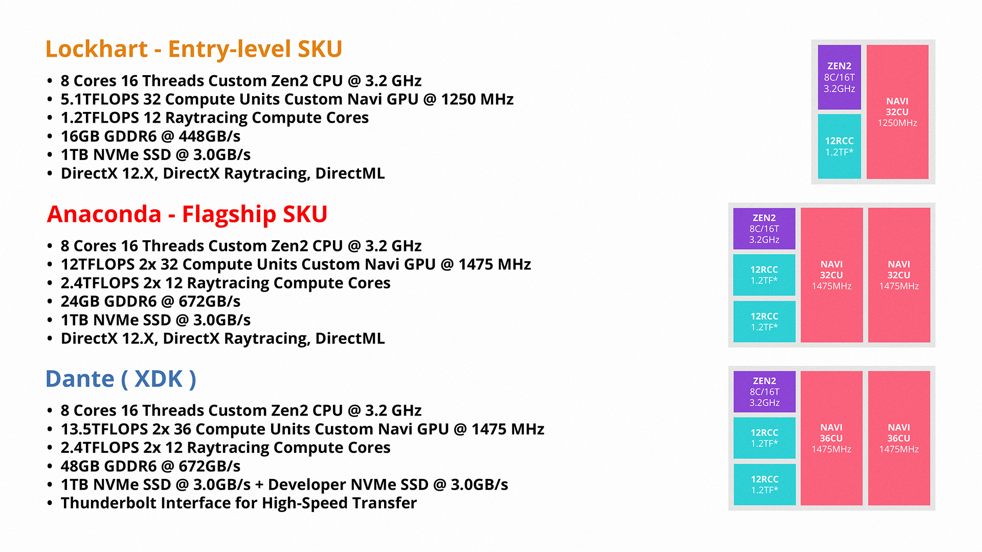
Anyone saw this?
Recently removed from /r/XboxOne
Why would Microsoft purposely downclock Lockhart's GPU? If anything, Lockhart should have faster clocks than Anaconda because of the better thermals (or less heat generated from having a single GPU chiplet design). Unless, Microsoft went with a super-shitty vapor/heatsink design for Lockhart, which I doubt.
Yield, Ppwer Delivery, Cooling, etc are all factors into price points; I'm not going to say this is legit just some factors to consider.Why would Microsoft purposely downclock Lockhart's GPU? If anything, Lockhart should have faster clocks than Anaconda because of the better thermals (or less heat generated from having a single chiplet design). Unless, they went with a super-shitty vapor/heatsink design on Lockhart.
My issue is with the RCC. Like it doesn't make mcuh sense to me, even if it were real and it did TF calculations, shouldn't it be closer to 60 TF?
Like lets make a simple comparison to the 2080RTX for instance. We see the performance with RTX on and RTX off. In DirectX Ray Tracing ,there is a flow chart section that says, if you have hardware enabled intersection go right, otherwise use a intersection shader and go left.
If we consider going left for a second, the developer needs to write an intersection shader, or whatever the case is. That shader has access to how many flops of 2080s 14? certainly that intersection shader can use up more than 1.2 TF of compute power. And assuming we see the difference of say 10 fps to 50 or 60fps, whatever that intersection hardware acceleration is doing, it's speeding up the process by that amount. So 1.2 TF doesn't make a lot of sense to me.
For reference point:
The full-fat version of Turing (it’s not clear which GPU this specifically refers to) is capable of 14 TFLOPS of FP32, 110 FP16 tensor FLOPS (that’s the half-precision mode) and 78 RTX-OPS. That last metric isn’t really a metric at all since we don’t really know what an RTX-OP is, exactly, but presumably, that kind of information will be fleshed out at a later date. The current Titan X, in contrast, is capable of 12 RTX-OPS.
So RT cores are doing about 6x more than what the intersection shaders on a Titan X are capable of. If this is my understanding.
This is either a plain wrong measure or the if it's indeed true, our understanding of the bottlenecks around triangle intersection is way outside our domain knowledge. I'd almost recognize that if ti's not compute power issues for figuring out intersection, then they should have invested in a lot more general compute power.
edit: Tom's Hardware made an attempt at a breakdown
https://www.tomshardware.com/reviews/nvidia-turing-gpu-architecture-explored,5801-10.html
So, given that…
FP32 compute = 4352 FP32 cores * 1635 MHz clock rate (GPU Boost rating) * 2 = 14.2 TFLOPS
RT core compute = 10 TFLOPS per gigaray, assuming GeForce GTX 1080 Ti (11.3 TFLOPS FP32 at 1582 MHz) can cast 1.1 billion rays using software emulation = ~100 TFLOPS on a GeForce RTX 2080 Ti capable of casting ~10 billion rays
INT32 instructions per second = 4352 INT32 cores * 1635 MHz clock rate (GPU Boost rating) * 2 = 14.2 TIPS
Tensor core compute = 544 Tensor cores * 1635 MHz clock rate (GPU Boost rating) * 64 floating-point FMA operations per clock * 2 = 113.8 FP16 Tensor TFLOPS
…we can walk Nvidia’s math backwards to see how it reached a 78 RTX-OPS specification for its GeForce RTX 2080 Ti Founders Edition card:
(14 TFLOPS [FP32] * 80%) + (14 TIPS [INT32] * 28% [~35 INT32 ops for every 100 FP32 ops, which take up 80% of the workload]) + (100 TFLOPS [ray tracing] * 40% [half of 80%]) + (114 TFLOPS [FP16 Tensor] * 20%) = 77.9
Yea... 1.2 TF for a RCC seems stupid. Won and done. That author should have googled tom's hardware
Last edited:
The 1.2TFlops value for the RCC can confuse at first, but only if you read it as Tera Flops as for a GPU.
In this context, TFlops means Tera First Lightray Operations for second.
For comparison, the TFlops of the RT cores in the 2080RTX is 3.27.
You serious?
lol no.. he's messing with you.You serious?
Nvidia only seems to have a specific number of 1 billion rays ~ 10 TF of compute performance.
the 2080RTX is capable of 10 billion rays, so approximately 100 TF of compute performance leveraging the ray tracing cores doing intersection and the like.
Even if 1.2 TF was representative of this number we'd still need the second number, which is the number of rays that are projected with 1.2 TF
- Status
- Not open for further replies.
Similar threads
- Locked
- Replies
- 9K
- Views
- 716K