
You are using an out of date browser. It may not display this or other websites correctly.
You should upgrade or use an alternative browser.
You should upgrade or use an alternative browser.
Next Generation Hardware Speculation with a Technical Spin [pre E3 2019]
- Thread starter AlNom
- Start date
-
- Tags
- 5 bytes non sequitur
- Status
- Not open for further replies.
Tkumpathenurpahl
Veteran
I'm an absolute HBM fanboy, so I'd be thrilled to pieces if it appears in the PS5.
http://www.guc-asic.com/upload/media/event/PDF/HBM_PHY_Controller_2018Q1.pdf
There is a company selling memory controller IPs promising hbm2 at 2.8gbps on 7nm for Q2 2019 (current IPs are 2.4 on 7nm, 2.0 on 16nm) That's a nice 716GB/s with only 2 stacks.
Once they get cheaper non-silicon interposers working with HBM, I wonder what the cost difference would be between two stacks HBM and 384bit gddr6.
I have questions:
What are the thermal management considerations of having the processing elements and the memory in such close proximity as opposed to spread out over a wider area?
What is the effect of different package sizes of HBM when it comes to presenting a level surface for good contact with the heatsink? I remember some inconsistencies with the early Vega cards based on from where the HBM2 dies were sourced (or was it where the final GPU was packaged?).
Last edited:
D
Deleted member 13524
Guest
Both.I remember some inconsistencies with the early Vega cards based on from where the HBM2 dies were sourced (or was it where the final GPU was packaged?).
Vega 56 used slower SK Hynix memory and was packaged without a resin filling around the dies. Vega 64 used faster Samsung memory and used the filling for higher/safer mechanical resistance. They were packaged at different places.
When custom AIB versions started coming out, things got mixed (Vega 56 with Samsung HBM, SK Hynix HBM reaching 1.9 Gbps, etc).
I'm an absolute HBM fanboy
You know you can get ahold of a HBM gpu right now, 16gb of it

Tkumpathenurpahl
Veteran
True, but I couldn't use it to play The Last Guardian or Spider-Man, so it'd just be an ornament. A beautifully beautiful ornament
Both.
Vega 56 used slower SK Hynix memory and was packaged without a resin filling around the dies. Vega 64 used faster Samsung memory and used the filling for higher/safer mechanical resistance.
I like this filling idea, let's brand it the LurpaK method, would go nice with some Hovis for a tasty PR piece
Next we can implement real thermal paste and call that Colman's (English mustard brand for non UK members) for that piquant finish to the new chip.
Perhaps I need more coffee and more importantly breakfast.
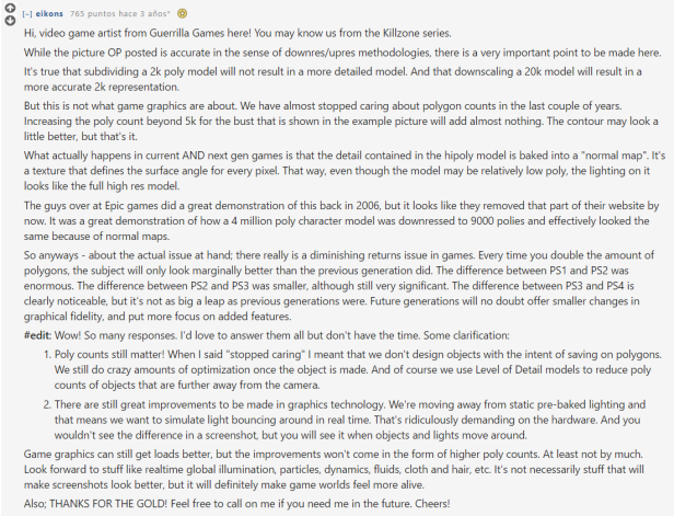
This is my own idea... all speculation and I am very lazy now to make an english version but it's understandable with Google Translator.
https://translate.googleusercontent...700248&usg=ALkJrhh8YU539ABjFbxFMRfcTRe1Hh_R9w
https://translate.googleusercontent...700248&usg=ALkJrhh8YU539ABjFbxFMRfcTRe1Hh_R9w
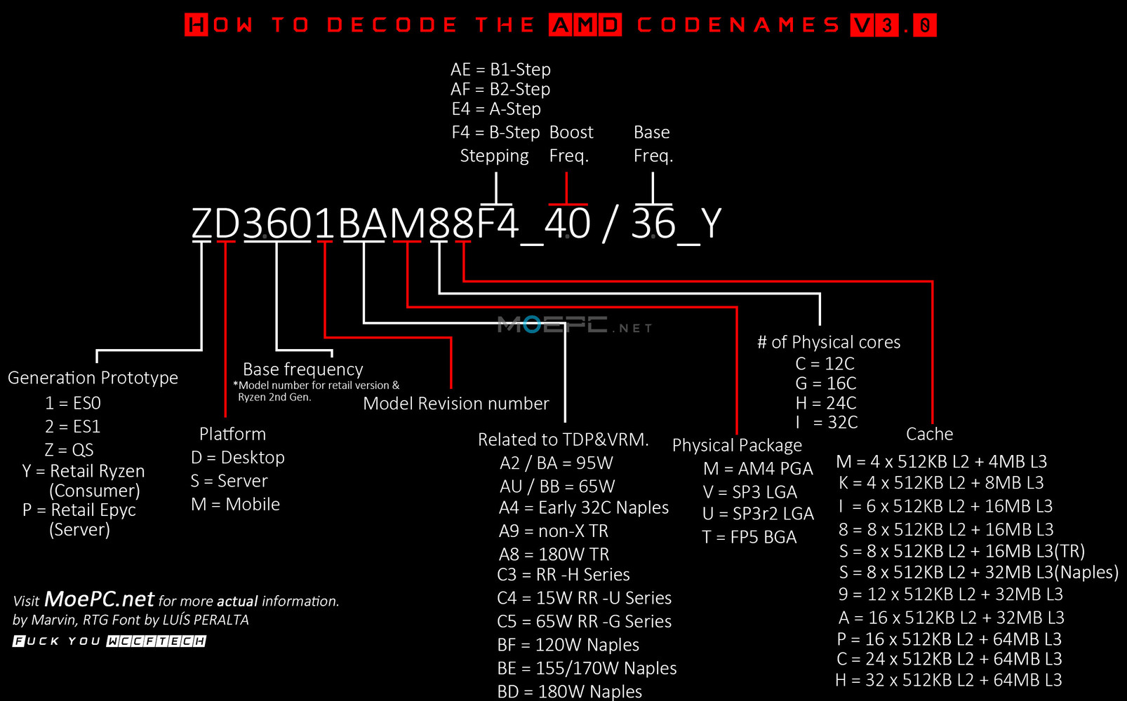
3.2Ghz boost clock/1Ghz base. Rather big difference between base and boost? Navi10LITE, mid range Navi i assume, even though LITE sounds like low power but why do that for a GPU?
Nice with 8 cores @3.2Ghz, if those are full cores and not like last time, that will probally the biggest jump over current gen.
Nice with 8 cores @3.2Ghz, if those are full cores and not like last time, that will probally the biggest jump over current gen.


Yes, thanks.
The tweet gets it wrong. The article explicitly states 1.6GHz base with boost to 3.2GHz according to the decoding scheme.3.2Ghz boost clock/1Ghz base.
Article isn't quite correct about Jaguar not supporting boost (puma has it) - not suggesting anything, but just uh... fact.
DavidGraham
Veteran
I like the part where an artist from Guerilla Games explains how next gen will focus on more real time GI, whether this is through ray tracing or other methods, remains to be seen.This is my own idea... all speculation and I am very lazy now to make an english version but it's understandable with Google Translator.
https://translate.googleusercontent...700248&usg=ALkJrhh8YU539ABjFbxFMRfcTRe1Hh_R9w
DavidGraham
Veteran
According to ComputerBase, they are Zen 2 not Jaguar.So Sony said fuck the CPU advances, give me 2x Jaguar cores, run them at 1.6 Ghz base clock, with boost speeds to 3.2 Ghz for Patched games for the PS5.
So Sony said fuck the CPU advances, give me 2x Jaguar cores, run them at 1.6 Ghz base clock, with boost speeds to 3.2 Ghz for Patched games for the PS5.
While GPU power is more important to gaming, i also doubt they wont abandon jaguar, hope they wont use it again atleast. Or sony will use the jaguar, aside from a ryzen cpu. The jaguar can double for BC and background tasks etc,
- Status
- Not open for further replies.
Similar threads
- Replies
- 21
- Views
- 1K
- Replies
- 22
- Views
- 7K
- Replies
- 18
- Views
- 2K
- Locked
- Replies
- 27
- Views
- 2K