I know that the HBCC seems to be more related to the HBM memory but at the same time my understanding is that it an important part to give the GPU the full coherent access to memory.
The idea is a GPU with 72 CU/NCU... ¿Reasons? PS3 was designed for 720P rendering in mind and it has 24 Texture Units, PS4 for 1080P (2.25x more) but it became rounded up to 3x and in PS4 we have 72 TMUs and 18 CUs. The jump from 1080P to 4K is 4X and this is the reason for this configuration. The other possibility is a 8*9 Configuration instead of a 6*12 configuration, but I prefered for space reasons the 6*12 Configuration.
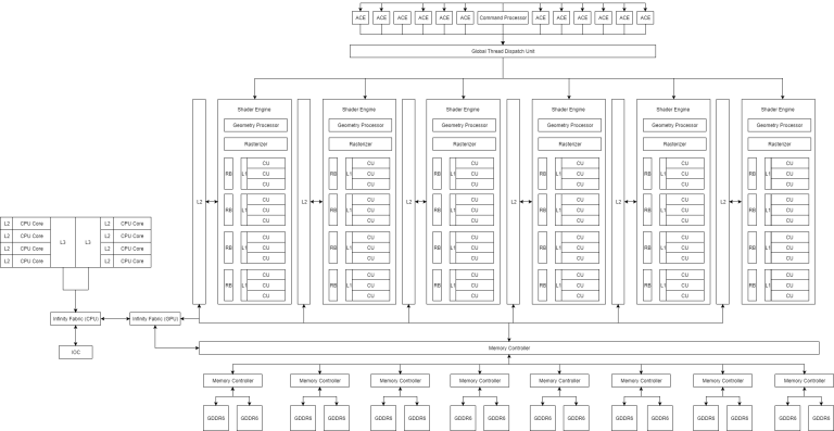
And well... As you have realized. The diagram is for an MCM unit where CPU and GPU are in different dies but with a common interposer, like the Wii U.
If this is just moving generic boxes around in a diagram, that's fine. It's such a high-level look that it's effectively saying "Zen+Vega" in picture form. I don't know if we can get much more out of it.
To clarify, Infinity Fabric is the data fabric. The data fabric box and the extra line between the CPU and GPU that are not for Infinity are redundant.
There is a control variant of the fabric, but items related to that are not represented in the diagram.
There would still be memory controllers between the HBCC and the GDDR6 in some fashion, since the HBCC itself doesn't control the memory channels in Vega.
Now that you've indicated these are not the same chip, I'm not sure if this arrangement matches what AMD would intend in a system with HBCC. Its proposals usually give the CPU its own DRAM, and give the GPU HBM. A CPU hanging off a separate GPU chip for memory is unexplored territory, since Zen has not shown itself capable of not having local memory.
Outside of Raven Ridge, which is one chip, AMD has only shown a form of "APU" where the CPU and GPU do not share an interposer, and the GPU gets HBM. AMD hasn't promised any significant level of connectivity between the CPU and GPU using an interposer, and hasn't shown that there's really a need since its existing non-interposer links seem more than sufficient for the CPU.
As noted, if this is Vega-based, the number of CUs per grouping stops at 3. It is true there is a shared instruction cache in that region labeled "L1", although that is just part of the shared hardware.
I'm not sure how much of the HBCC is needed for a console, or if the GPU is the sole owner of all the memory in this case.
I have a feeling the CPU and system overall may not align with that concept without some significant work, since a slave device that cannot process certain system/link errors that could interfere with communication with the CPU owns the memory needed to process errors.
I'm not sure using TMU count or target resolution is the best metric for improvement, and it misses the massive growth in other resources and the fact that the texture units were higher-clocked and more capable with the current generation. Also, if this is 7nm or the like, a chip that is not significantly more endowed than Vega may be small enough that a 512-bit GDDR6 bus may be difficult to fit (roughly the size of 256-bit Polaris 10), and an interposer doesn't help GDDR6 or the CPU. It makes having an interposer rather questionable since this setup is not offering new integration capability.
If clocked like Vega at ~1.5 GHz (may be a bad idea), it could get something like the 8x FLOP boost over the prior generation like the PS4 did, but less of a gain versus the Pro (~3x) or Scorpio(~2.4x). It may not be able to cleanly differentiate itself as a new generation. (edti: This may be unavoidable and not a problem with this specific concept in particular.)