DavidGraham
Veteran
So same as FuryX?• 4 triangles per clock
So same as FuryX?• 4 triangles per clock
Thanks Rys, I really appreciate it. Going to put it into good use")
From the pure spec-sheet numbers - yes.So same as FuryX?
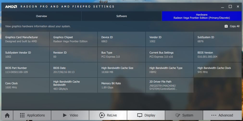
They also mention another AMD GPU on SiSoftware with 1536 SPs and a 1024-bit bus, and is associated with Kaby Lake.According to the data from CompuBench, WX 9100 would have 1792 cores more than WX 7100. The listing reveals that WX 9100 has 64 Compute Units (4096 Cores) and a maximum clock of 1200 MHz. Listed global memory size is definitely pointing towards 16GB configuration, so this would be sixth Vega with such memory size.
So this lends credit to the theory that more triangle rate is dependent on the optimizations made through primitive shaders, which should be application specific, and not transparent.From the pure spec-sheet numbers - yes.
Gut feeling or behind the scene info?RX Vega will be comparable to Radeon 9700 in terms of impact.
I think I remember PXAA being an old modified FXAA filter, it should have a temporal component as well called TPXAA.New(ly added) antialiasing mode incoming as well?
PXAA
So Vega pure Pro cards will be slower but come with certified drivers? Well there is one distinction alright.From Videocardz: "AMD preparing Radeon Pro WX 9100 with Vega GPU."
Wether or not I have one or the other or both would be subject to confidentiality agreements between two or more of the following parties: Me, my gut and AMD.Gut feeling or behind the scene info?
Wether or not I have one or the other or both would be subject to confidentiality agreements between two or more of the following parties: Me, my gut and AMD.
But just think about it, it only makes sense.
9500 Pro's didn't mod to 9700 Pro, 9500's did (if they had the memories in "L" pattern around the chip instead of one row like 9500 Pro)Did we get so much secrecy before R300 launch? I don't remember any leaks for R9700 from that era and was totally blown away by that card at a time! Best I could afford was poor man's version, aka Radeon 9500Pro which unlocked to 9700Pro! Still have one R300 card in my collection
Compared to? GeForce 4600 Ti was longer, but the difference was insignificant. Custom models of GeForce 4800 Ti introduced shorter designs, which were comparable to Radeon 9700 PRO9700s were gpus which needed smaller boards
Radeon 9700 PRO had power connector, GeForce 4600 Ti didn't have.and they were less power hungry
Radeon 9700 PRO was based on the same process as GeForce 4600 Ti. Later released FX brought newer process. I think current situations is similar, Vega is based on older process (14nm) than upcoming Volta (12nm).and they were built on the n-1 node.
Wether or not I have one or the other or both would be subject to confidentiality agreements between two or more of the following parties: Me, my gut and AMD.
But just think about it, it only makes sense.
Yeah I can see how you're saying that from all the reviewers benchmarks and design testing we've seen.It makes sense, but only if Pascal has the role of R300 and Vega is the FX5800. Then we could say it is late, loud and low performing.
Looks like they forgot to change memory into HBC at one point.
edit: possible explanation, why 8 GiByte HBM2 stacks were not in SK Hynix product catalogue or a simple readout-bug.
<blockquote class="imgur-embed-pub" lang="en" data-id="a/1AO2C"><a href="//imgur.com/1AO2C">gpu-z</a></blockquote><script async src="//s.imgur.com/min/embed.js" charset="utf-8"></script>
Hence „possible“.Or neither. Raja did confirm they are using multiple HBM sources.