HBM Thread

PC Watch has a nice article and slide deck on the first generation of Hybrid Memory Cube tech.
That is another stacked memory, not the High Bandwidth Memory in the article.

Thanks for the link, will read now.

After "reading" the google translate, some of the key info is;

1st gen HBM will come in 1GB blocks, running at 1Gbps providing 128GB/s bandwidth and should be on the market ~Q2/2015.

2nd gen HBM will come in 1GB, 2GB, 4GB blocks, running at up to 2Gbps providing 256GB/s bandwidth with production starting in Q2/2016.

The maximum(?) number of blocks per GPU/CPU/SoC is 4, so 1st gen HBM will be up to 4GB and up to 512GB/s while 2nd gen HBM will be up to 16GB and up to 1024GB/s.
There is also a roadmap to increase memory speed to 3Gbps which will take maximum bandwidth up to 1536GB/s.

Hynix have listed an 8GB version using twice the amount of DRAM layers(8-hi compared to the standard 4-hi) with production starting in Q2/2016.
 
Last edited by a moderator:
That is another stacked memory, not the High Bandwidth Memory in the article.

Thanks for that; I coulda sworn that AMD was part of that consortium, but I guess not. AMD is a big deal when it comes to memory design as GDDR5 is a popular industry standard. I wonder if there will be GDDR6, and how many industry members will opt for HBM over HMC or if they're supposed to occupy separate niches / be much more device specific than some interchangeable standard.

For 1st gen, 4 x 1 GB seems only large enough for GPUs. I wonder if the first gen might more like an extra tier of cache in some configurations.
 
Last edited by a moderator:
Thanks for that; I coulda sworn that AMD was part of that consortium, but I guess not. AMD is a big deal when it comes to memory design as GDDR5 is a popular industry standard. I wonder if there will be GDDR6, and how many industry members will opt for HBM over HMC or if they're supposed to occupy separate niches / be much more device specific than some interchangeable standard.

For 1st gen, 4 x 1 GB seems only large enough for GPUs. I wonder if the first gen might more like an extra tier of cache in some configurations.
A quick google gave me this;
HMC
One advantage of HMC is that it allows Micron to preserve its business model and deliver a packaged memory to a customer
HBM
Unlike HMC, it is designed for 3D IC integration and can integrate on an interposer only, which interfaces with a CMOS I/O interface. Rather than selling a packaged part, manufacturers of HBM will be essentially selling bare die to be mounted on an interposer.
Source.
 
Got it. HBM makes sense for consumer parts, most people are never going to upgrade memory before they upgrade their entire computing unit. AMD might start marketing svelte whole system APUs on graphics card like form factors with substantial cost and performance improvements. It would reduce the fun of building your own system by just a bit more though.
 
Of note is that HMC has less shine to it if you have your own in-house high-performance memory controller designs, since much that is taken up by the base die controller and outside of your control.

AMD, Intel, and Nvidia are not noted as being members, from what I've been able to find.
 
Some info related to HBM...

sys-plus-3.jpg


http://electroiq.com/insights-from-leading-edge/wp-content/uploads/sites/4/2016/03/sys-plus-3.jpg


sys-plus-2.jpg

http://electroiq.com/insights-from-leading-edge/wp-content/uploads/sites/4/2016/03/sys-plus-2.jpg
 
AMD, Intel, and Nvidia are not noted as being members, from what I've been able to find.

I thought Intel was one of the driving forces behind HMC. The advantage of HMC over HBM is the vastly increased memory capacity possible, the downside is higher power consumption (because of the high speed signalling).

Cheers
 
I thought Intel was one of the driving forces behind HMC.

The post you quoted is more than three years old. Altera was always/is still listed as a Developing Member of the HMC Consortium, just with the added tag "Now part of Intel".

Still neither Nvidia nor AMD among the listed adopters.
 
I thought Intel was one of the driving forces behind HMC. The advantage of HMC over HBM is the vastly increased memory capacity possible, the downside is higher power consumption (because of the high speed signalling).

Intel and Micron worked together on HMC, which at this point is one of a number of shared initiatives in memory between the two. Intel had some of the early deployments, although it remains off the member list of the HMC consortium outside of its Altera division.
Perhaps its partnership with Micron and ground-floor presence for the tech makes explicit membership unnecessary. If it has need to steer the shared standard, it could have say via Micron--or it may not have the need to follow the standard.
Intel in this case may be so embedded in this tech that it loops back around in terms of wanting more control over its own destiny. Knights Landing's MCDRAM is described as an iteration of HMC customized by Intel.
 
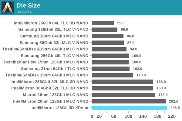
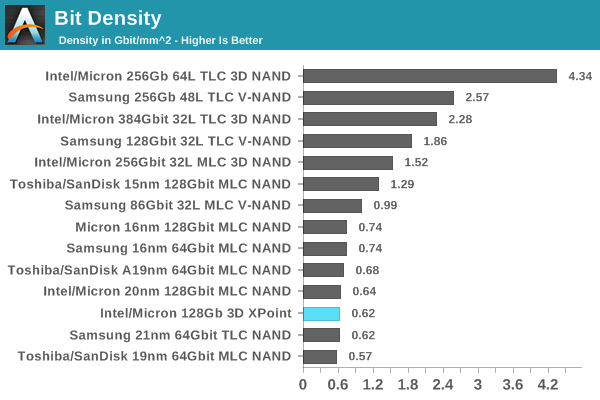
It looks like this thread is dedicated to modern high bandwidth techniques rather than HBM, specifically, so I think TechInsights' 3D XPoint article might be useful to share for those that missed it.

http://www.techinsights.com/about-t...int-memory-die-removed-from-intel-optane-pcm/

Anandtech did a nice high-level summary for laypersons. I know I appreciate it. :p

http://www.anandtech.com/show/11454/techinsights-publishes-preliminary-analysis-of-3d-xpoint-memory

73111.png


66757.png


TechInsights calculates that 91.4% of the 3D XPoint die area is occupied by the memory array itself. This is a much higher figure than for NAND flash, where the record is 84.9% for Intel/Micron 3D NAND with its "CMOS under the array" design that puts a large portion of the peripheral circuitry underneath the memory array instead of alongside. Samsung's current 48-layer 3D V-NAND manages an array efficiency of just 70%, and 3D NAND from Toshiba and SK Hynix has been comparable. This means that once Intel gets around to increasing they layer count in future generations of 3D XPoint memory, they should be able to get much closer to the ideal capacity scaling than 3D NAND memory can currently achieve.

The analysis from TechInsights confirms that 3D XPoint memory is manufactured using a 20nm process, with the same pitch in both the bitline and wordline directions of the memory array. The DRAM market is only just moving beyond this milestone, so comparing the density of 3D XPoint to current DRAM highlights the fundamental capacity advantage 3D XPoint enjoys: around 4.5 times higher density compared to typical 20nm DRAM, and about 3.3 times higher than the most advanced 1Xnm DDR4 on the market. This gap is likely to widen with future generations of 3D XPoint.
 
Back
Top