AMD Vega 10, Vega 11, Vega 12 and Vega 20 Rumors and Discussion

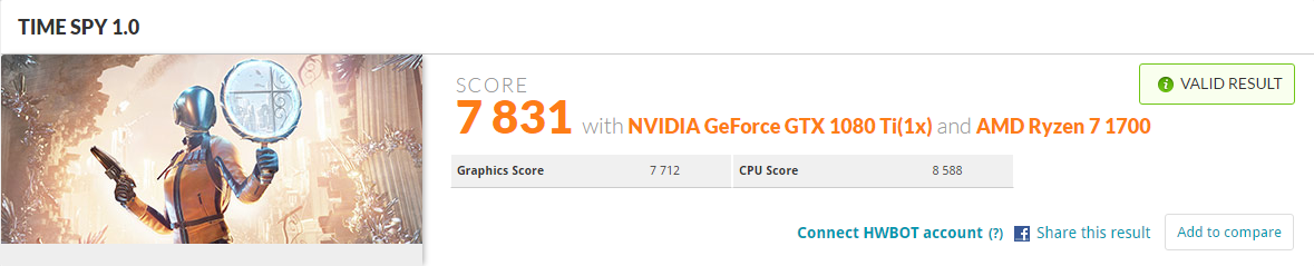
If that's at stock then that's a good improvement since the benchmark was released, I guess most of the benches I looked at were at the benchmark's release or pascal cards' because many recent user benches come up with 5.2k-5.3k as opposed to 5k+ from last year.

https://www.overclock3d.net/gfx/articles/2016/07/16120648644l.jpg

http://www.overclock.net/content/type/61/id/2829273/

https://www.extremetech.com/wp-content/uploads/2016/07/timespy-3.png

Hopefully the 80% of AMD driver team's workhours get similar gains for Vega before release because right now it doesn't look nice even for 1.2Ghz.
 
The score is pretty much spot on for what Fury X @ 1,2 GHz should get, so sounds like OC'd Fury X and nothing else.
 
Except for the 700Mhz memory clock(but it could be the idle clock doubled) and most importantly, the 8GB of vram. The driver version is also perhaps not a public driver.
 
thanks to the sharp eyes of GeniusPr0 who spotted that the Device Hardware ID for the entry is 687F:C1, and that leads to a story we covered back in December.
...
We also noticed that ID for a Doom Vulkan result set that was posted from an AMD event (check photo above) So yes, chances are getting much higher that this is the real thing. You can retrieve the Hardware_ID info once you place the result set into a comparison. You then will also notice that this result set was a fresh one, created on the 12th of April.
http://www.guru3d.com/news_story/possible_radeon_rx_vega_3dmark_time_spy_benchmark_result.html
 
Pretty much confirms it then, reddit user ibomby has been saying that the Vega pci id is 6860 even before Polaris 12 showed up so maybe the higher clocked version is not the same id this time like it was for Polaris 10. But even for a 1.6Ghz core clockspeed, it'd barely scrape past a 1080 if the time spy score is any indication.
 
Pretty much confirms it then, reddit user ibomby has been saying that the Vega pci id is 6860 even before Polaris 12 showed up so maybe the higher clocked version is not the same id this time like it was for Polaris 10. But even for a 1.6Ghz core clockspeed, it'd barely scrape past a 1080 if the time spy score is any indication.
At least one Vega model is known to be 687F:C1 since late last year (Doom demo)
 
At least one Vega model is known to be 687F:C1 since late last year (Doom demo)
And this is the ID of the GPU in that Time Spy score, so could this be a cut down Vega?

index.php
 
It's not cutdown chip, compubench shows 64 compute units.

https://compubench.com/device.jsp?benchmark=compu20d&os=Windows&api=cl&D=AMD+687F:C1&testgroup=info

It can be the underclocked version like last year's Polaris 10 id at 800Mhz while the other was at 1266Mhz. But they had the same pci id but were different in the "revision" number. This time for Vega 10, 687F has shown up with two "revisions" but both are similarly clocked at 1.2Ghz and not 1.6Ghz one would expect after AMD's MI25 announcement.
 
I'll try to match the exact tflop number (9.8 something) and run Time Spy on my 1080 Ti so we can see if there's any improvement in comparable theoretical perf. I'm running a Ryzen 1700 so the CPU part should be comparable.
 
Pretty much confirms it then, reddit user ibomby has been saying that the Vega pci id is 6860 even before Polaris 12 showed up so maybe the higher clocked version is not the same id this time like it was for Polaris 10. But even for a 1.6Ghz core clockspeed, it'd barely scrape past a 1080 if the time spy score is any indication.
With the 700MHz HBM it has bandwidth less than 360 GB/s (comparable to the 256bit 11Gbps GTX 1080). That should be the most limiting factor. Top model with full-speed memory should have 43 % higher bandwidth.
 
Even with older drivers if they were really just matching Fiji clock to clock, they surely would have scratched Vega altogether - so there must be another explanation
 
With the 700MHz HBM it has bandwidth less than 360 GB/s (comparable to the 256bit 11Gbps GTX 1080). That should be the most limiting factor. Top model with full-speed memory should have 43 % higher bandwidth.

http://www.3dmark.com/3dm/19646173

This is with -502 memory clock (the maximum I could downclock via Afterburner), total b/w 440.4 GB/s and I dropped a bin on the core clock to 1367 (at 0.800mv voltage) to give the theoretical advantage to the Vega GPU. Starving the GPU from mem b/w did decrease the score but not dramatically in this case. Also fair to note that at these clocks and voltage the 1080 Ti was consuming an average of 130 watts with a maximum of 150.
 
Last edited:
and not 1.6Ghz one would expect after AMD's MI25 announcement.
That 1.6Ghz number was derived from the calculated 12.5 TFLOPs for the MI25, AMD never gave a solid number for that card though. Not for the FP16 or FP32 throughput, instead people calculated that from this slide:


AMD-INSTINCT-VEGA-2-840x473.jpg


400 Petaflops /16 MI25 GPUs = 25 TFLOPs FP16
It also matches the name MI25, though there is the possibility AMD used approximative numbers for everything. I guess this could be an engineering sample with much lower clocks or the MI25 is a dual GPU part.
 
Even with older drivers if they were really just matching Fiji clock to clock, they surely would have scratched Vega altogether - so there must be another explanation

The saving grace could be that the drivers are for compute and not gaming, testing out the pro-version on a graphics benchmark for the heck of it. Most of the other benchmarks were on compute related sites.

There don't seem to be any improvements over Fiji or it even seems to have regressed, especially on the second test where nvidia do better and hence might be influenced by the front end performance. It would be pretty terrible if AMD still have to have better TFLOPs numbers to match an nvidia card since GP102 would remain head and shoulders above AMD's best then.
 
The score is pretty much spot on for what Fury X @ 1,2 GHz should get, so sounds like OC'd Fury X and nothing else.
Which is exactly what's expected from a 14nm FuryX. Which also means all the bullet points on slides and larger than expected die size, despite cutting a geometry stage as indicated by drivers, didn't amount to anything. The slowest Hynix HBM2 isn't being used to its fullest. A redesigned NCU for higher IPC and clockspeeds better mean more than just 14nm. Packed math shouldn't take that much area, which is why it's beneficial.

Still can't help but think we're looking at a Vega11 or mobile design, even if running on Vega10 silicon and limited by drivers. These figures would seem to confirm AMD is indeed sandbagging. Even Polaris with a few more cores would have surpassed this performance.
 
AMD never sandbags, and just a question, how many Fury X's have ever gotten to 1200 mhz?

thought it never had that much head room. Also AMD's higher CU frequency, guess what we have no clue what they are comparing it to, I highly doubt its Polaris, cause they tend to compare to 2 or 3 generation old products when making comparisons.
 
That 1.6Ghz number was derived from the calculated 12.5 TFLOPs for the MI25, AMD never gave a solid number for that card though. Not for the FP16 or FP32 throughput, instead people calculated that from this slide:


AMD-INSTINCT-VEGA-2-840x473.jpg


400 Petaflops /16 MI25 GPUs = 25 TFLOPs FP16
It also matches the name MI25, though there is the possibility AMD used approximative numbers for everything. I guess this could be an engineering sample with much lower clocks or the MI25 is a dual GPU part.


Well for what its worth they dropped the TFlop amounts for the MI125 to under 12, and also its a 250 + watt TDP and one slide even says 300 watts, so it might be burning quite a bit more than the 225 watts we have seen with Vega.
 
3R1W would read 3 registers and write 1 in a single cycle. There may be a delay if swizzling within those registers as the data shifts according to the DPP patterns. Flipping along powers of two with write masks.

Realistically it's probably 5R2W with the extra ports servicing LDS or scalar instructions.
A bit late to answer, but anyway, here are my 2 cents to that:
4 or even 7 ports on the vALU register files sound absurd to me. Additional ports cost significant area (and power). 16MB of vector register files (256kB per CU) in Fiji (and Vega10) would be pretty much out of reach. Given the high density of the SRAM used for the register files it's entirely possible (I would say even likely) that each register file has exactly a single (shared read/write) port,i.e. it's normal single ported SRAM. That's completely enough to ensure there are no conflicts for vALU operations with proper pipelining (stretched out over at least three instructions). If some memory (including LDS) instruction needs some additional register bandwidth, the scheduler in the CU could "steal" an access cycle from instructions with only two source operands or it has to create a bubble in the vALU pipeline. Already a dual ported register file would actually surprise me.
 
Back
Top