
You are using an out of date browser. It may not display this or other websites correctly.
You should upgrade or use an alternative browser.
You should upgrade or use an alternative browser.
The 6-core SKU will be salvaged 8-core die.
Apparently with Ryzen, AMD is following the same "macro-block" strategy with Jaguar, of tightly packed modular quad-core clusters. The difference this time is that CCX is expandable to multiple dies and sockets.
I guess native Ryzen quad-cores will come only as APUs.
Apparently with Ryzen, AMD is following the same "macro-block" strategy with Jaguar, of tightly packed modular quad-core clusters. The difference this time is that CCX is expandable to multiple dies and sockets.
I guess native Ryzen quad-cores will come only as APUs.
Infinisearch
Veteran
Where did you read this?they could help clear out L3 pressure problems findings.
In this case AMD needs to fix their drivers. I'd assume Windows also uses this API internally to guide scheduling. We could see performance improvements as result even without software patches.Thats what CoreInfo uses, there's already a few posts about that & Ryzen seems to give wonky results with each thread reporting separate dedicated L1, L2 & L3.
That said, AMD has aimed low with just four cores for a shared L3, on top of that, Ryzen seem to have a weak inter-CCX fabric, which boggles the mind given how cheap on-die bandwidth is. This makes it much more sensitive to pathological scheduling cases.
Should the fabric be strong enough, the protocol and architecture may not be designed to leverage it. Intel's MESIF came about as part of its creation of the ring bus and LLC, and those two features provide a fair amount of bandwidth amplification and absorb snoop traffic. It starts to falter in higher counts, but it has some nice behaviors until then.
MOESI, at least as we know it, is older and doesn't derive as much read amplification from on-die storage. It should save writes back to DRAM when sharing dirty lines relative to MESIF, but then Ryzen's lack of an LLC could force the so-called savings in that scenario to incur coherence broadcasts and writes back to the home node like this was a multi-socket system.
What this might offer, however, is simplifying the scale-up to larger chip counts. The system doesn't try to track as many lines capable of sharing clean data, and dirty lines write back to the home node more quickly in the absence of single-die optimizations. If there's something like HT assist, the interchange of snoops and data would be simplified at the cost of chaining the fabric to the memory controller's throughput--which per Vega's GMI fabric and elsewhere is described as being the case.
The price of scalability is per the usual that performance per granule and at lower counts is the poorer for it.
In Vega's case it's described as a positive that the interconnect is equal to memory bandwidth, although interestingly Naples is confirmed to be able to connect to Radeon Instinct cards with GMI (presumably the MI-25). It would have been interesting if Ryzen were able to do something similar as a value-add.
Another area of scalability at the cost of effectiveness may be AMD's turbo and XFR functionality. They perhaps benefit some kind of data center load with a VM per CCX or sustained multisocket load. Either it's some rather coarse turbo bins for a limited subset of cores for spiky loads, or the relatively fixed all-core turbo a significant ways below. The case with a few highly active cores and the rest being mostly but not fully parked is not handled all that well compared to what Intel can do and may match games more than other applications.
A question then for these multi-die solutions is if the power delivery and clocking scales up, such that Ryzen's significant loss of clock speed with more than 2 cores active actually translates into 8 cores with the equivalent of a quad Ryzen, or if it's actually 2 cores per package.
The millisecond polling for AMD's power management is in some ways a bit slow, possibly to allow the MCM to coordinate?
AMD's prior interconnect started with the first dual-core A64s, and lasted in some form until Zen--theoretically. Jim Keller's presence at AMD sort of book-ends the lifespan of a really creaky interconnect.This seems to be a given. Intel changed their fabric topology and properties multiple times when they started to scale beyond 4-cores. Current one is the result of many iterations. AMD clearly is behind in this area.
Anarchist4000
Veteran
Keep in mind AMD should be a mesh, not a ring. The inter-CCX fabric is probably adequate, just not for low node count designs. Smaller systems favoring Intel's ring, larger favoring AMD's mesh. How many links they support being an interesting question. At scale, I'm guessing they were going for SUMA, not NUMA.It should be said that it is Intel's Xeons,which have a dual ring L3 systems, that offers COD, - and up to 12 cores per cluster. They also offer much higher bandwidth on the LLC ring bus.
IMO, this will hurt AMD in workloads with varying amounts of active threads. The OS scheduler will have an impossible task. If so, I'd expect Ryzen 2 to have a much stronger inter-CCX fabric.
You can't look at the past and use the previous experience of going from 2 to 4 core to say how things will be. These are different times and if you don't already know technology evolves exponentially not lineally, if we had to wait 13 years to use 4 core than doesn't mean we will have to wait another 13 to use 4 that is not how the technology world works.
In the past the developers focus and learn how to use multicore of different architectures than x86, a studio with years of experience in using multi core in CELL doesn't use any of that knowledge for their games in PC, now its different not just that studies learn how to code for x86 but also have more freedom in what they can do with vulkan and dx12. I am sure we will see games using more than 4 cores in a year or 2 thats just where the industry is aiming.
Also zen stock was about a million of cpus and its almost all gone so yes the demand its pretty high and will be in the future, this is not BZ in any sense this is something new with a bright future in front of it.
Regarding L3 and CCX, if Ryzen 1600X and 1500X are three cores per CCX, they could help clear out L3 pressure problems findings. But if they are 4+2, the waters will be much more muddy.
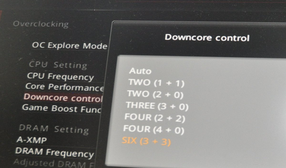
My understanding is that both CCXs must have the same number of cores active.
Some sites have simulated the 1600X (and 4-core) performance using a BIOS feature.
http://www.phoronix.com/scan.php?page=article&item=amd-ryzen-cores&num=3
http://www.pcgameshardware.de/Ryzen-7-1800X-CPU-265804/Tests/Test-Review-1222033/#a5
hoom
Veteran
So it is likely to have been an AMD booboo? People have been blaming MS but it seemed like AMD to me.In this case AMD needs to fix their drivers. I'd assume Windows also uses this API internally to guide scheduling.
Do you know what actually gives the response? (hardware, BIOS, drivers, some OS 'known hardware' file?)
So it is likely to have been an AMD booboo? People have been blaming MS but it seemed like AMD to me.
Do you know what actually gives the response? (hardware, BIOS, drivers, some OS 'known hardware' file?)
It is AMDs they didn't work with devs to show their CPU before launch so anybody had an idea of what to do. Why after the BZ fiasco AMD didn't learn that you should optimize before launch so it doesn't hurt the image of the product is beyond anyone undertanding
My understanding is that both CCXs must have the same number of cores active.
Some sites have simulated the 1600X (and 4-core) performance using a BIOS feature.
http://www.phoronix.com/scan.php?page=article&item=amd-ryzen-cores&num=3
http://www.pcgameshardware.de/Ryzen-7-1800X-CPU-265804/Tests/Test-Review-1222033/#a5
Yes you need to hace equal number of core active in each CCX this pic shows the possible configurations.
MESIF came about as part of its creation of the ring bus and LLC, and those two features provide a fair amount of bandwidth amplification and absorb snoop traffic.
MOESI, at least as we know it, is older and doesn't derive as much read amplification from on-die storage
As I see it, they serve different purposes.
Without the Forward state, each cache with a line in state Shared responds with data on a read probe. With many caching agents the requesting node can be flooded with the same cacheline data from every cache that has the line in Shared state. With MESIF, only the cache that has the line in state F responds with data.
The Owned state allows a core to broadcast writes to a cacheline to all cores which has the cache line in the Shared state. Without the O state a write to a cacheline invalidates all other copies of that cacheline which then has to be requested explicitly on subsequent reads from other cores.
The addition of the F state reduces bandwidth requirements when multiple cores reads shared lines. The addition of the O state improves latency on cores which holds the cacheline in the S state because they avoid a cache miss. I see F as a read optimization, O as a write optimization (in particular for cachelines in producer-consumer relationships).
The CCX interface acts as coherency agent for all the cores in the CCX, so a read probe from a core in a different CCX only gets one response even if all four cores in the CCX has a copy in the S state. The motivation to add the F state is thus low, especially since it puts extra pressure on the main memory system when the F state is lost.
The fact the L3 is a victim cache also plays into this. The odds of finding a cache line in the L3 in a different CCX is low, since it only holds data spilled from its own cores; Except of course the case where the OS scheduler shuffles processes around with gay abandon. Inter-CCX shared data is thus likely to be found in the L2s, and again, here the response bandwidth is reduced by a factor of four because the CCX interface filters the response.
Cheers
It is the case with MESI that a Shared line can forward data read request, which seems like a scaling barrier once multicore chips became more common.As I see it, they serve different purposes.
Without the Forward state, each cache with a line in state Shared responds with data on a read probe. With many caching agents the requesting node can be flooded with the same cacheline data from every cache that has the line in Shared state. With MESIF, only the cache that has the line in state F responds with data.
In MOESI, Shared does not forward data.
For MOESI, a write to the cache line is going to invalidate other copies. The Owned state allows Modified lines to be shared without writing back to memory, reducing writes. The Owned state tracks who is responsible for the final update, a write to a line that has copies elsewhere is going to invalidate any other shared copies, which is true for Owned and Shared. When exactly a dirty line is forced to write back is unclear, some descriptions such as from http://www.realworldtech.com/common-system-interface/5/ indicate that any transition for an Owned line is going to write something back. This is more restrictive than the wiki description of MOESI, since an O to M would seemingly be possible without a writeback (still needs invalidates). Perhaps the RWT description oversimplified the O-M case, unless AMD is very conservative with the O state. The wiki description seems to involve some operations that may not be implemented or common (write broadcasts rather than invalidates, and a writeback that converts O to S without eviction).The Owned state allows a core to broadcast writes to a cacheline to all cores which has the cache line in the Shared state. Without the O state a write to a cacheline invalidates all other copies of that cacheline which then has to be requested explicitly on subsequent reads from other cores.
Snoops may provide the cache with information that a line is shared elsewhere, which helps determine if the line should be S or E, but those other S lines do not provide data.The CCX interface acts as coherency agent for all the cores in the CCX, so a read probe from a core in a different CCX only gets one response even if all four cores in the CCX has a copy in the S state.
Anarchist4000
Veteran
Trivial, but may have been a design decision. The problem goes away as they add nodes and a GPU/APU is likely to add nodes. Vega with 32 PCIE3 lanes, that likely substitute for IF links, makes it half a Naples. 8 core Ryzen's being the other half. Memory distribution is a bit unknown at this point. It could have been an oversight, or they didn't feel like fabricating two similar, but slightly different parts. Likely would come at the cost of some PCIE lanes as well.Is it non-trivial to double the inter-CCX link on a dual CCX design? Seems like low hanging fruit for Zen 2 consumer version.
Active, but not necessarily scheduling anything. So long as they don't reserve cache, they could all be enabled with 3 idling as to not consume resources.Yes you need to hace equal number of core active in each CCX this pic shows the possible configurations.
hoom
Veteran
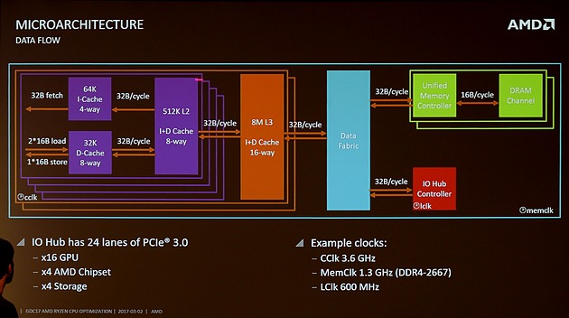
32Bytes/clock everywhereIdk if this image was posted before:

Confirms inter-CCX @ ram clock.
Arrows indicate 32B/clock full duplex but shared with other traffic so thats certainly a bottleneck if there is a lot of inter-CCX traffic.
What is the BW of QPI? i heard it was similar32Bytes/clock everywhere
Confirms inter-CCX @ ram clock.
Arrows indicate 32B/clock full duplex but shared with other traffic so thats certainly a bottleneck if there is a lot of inter-CCX traffic.
Bumped into some discussion about Ryzen scheduling bug in Twitter (some links, but not much new info):
https://twitter.com/MicrosoftHelps/status/839581647351738375
https://twitter.com/MicrosoftHelps/status/839581647351738375
Similar threads
- Replies
- 90
- Views
- 13K
- Replies
- 220
- Views
- 87K
- Locked
- Replies
- 24
- Views
- 14K
- Replies
- 601
- Views
- 88K