Nvidia Pascal Announcement

Thanks Steven, those numbers were about 2x above my expectations aswell. I guess it goes to show how Nvidia has been dominating the HPC accelerator market.

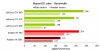
So in the whole of 2016, gaming revenue was a total of 2818 M $ and HPC was 339 M $, so that would constitute about 12.02 % of the gaming revenue.

This is definitely not peanuts to Nvidia as I previously stated!

Now, given that the Pascal architecture cost something like 2500 M $ in RnD* to develop, it would take the Tesla/HPC segment about 7 years to accumulate that sort of revenue (less if growing trend continues), do you think Nvidia can afford to build an architecture specifically for HPC only? No, of course not.

HPC is still riding piggyback, maybe this will change with the surge of deep learning applications? It looks to be a huge new market.


* I was told this number by nvidia architecture chief, is there a better official number?
You know that R&D budget is rather diverse and not all of it is hardware, also Pascal R&D would also includes the massive amount spent on auto/Tegra X2/etc.
But even then it does not matter because all sales segments-markets profit (this comes down to margins) contributes to R&D even if it is different HW.
Also part of this is building for the future, the value of HPC-ML-auto is meant to be massive but time will tell.
To see how well HPC and ML influences growth and revenue you need to watch it from Q3 FY16 onwards, due to the various projects coming on-line or new ones signed since P100 released.
Also do not forget profit margin.
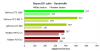
The GP102 is $1200 (and trend shows only around 1% goes to consumer), the cheapest PCIE GP100 card is around $5,300 and the largest projects can be direct sales (meaning all margins go to Nvidia and none shared with sales channel partners/integrators such as Cray).
So factor that in your revenue, especially as even the higher profit margin gaming cards only have a consumer demograph of 0.8% to 1% each historically; that is the 980 and 980ti and also Titan X.
So greatest revenue in gaming is from the lower margin models while net profit between segments would be much closer.
The interesting slide would be profit for each segment-market.
Just from a HW context it could be seen HPC generates 3x to 4x more profit margin (yeah generalising not usually a good idea I agree but it is going to be high), but this is made more complex by 'soft costs' of software, which is applicable to both HPC-ML and gaming in different ways but optimisation-API-libraries-coding teams exist in each.
Cheers
 
Last edited:
Looks to me like the RnD on average the last 3 years was around 300M / quarter or 1200 M per year. so that would be 3600 M over 3 years development, seems fairly reasonable that the Pascal could suck a good 2-2500 M.
Again, considering how close Pascal is architecturally to Maxwell and that Volta is supposedly much more different and is already spoken for for several supercomputers and hence is on a tight schedule I would expect that even graphics R&D was about split between Pascal and Volta. But 3 years ago also overlaps with Maxwell development (Gen 2 released less than 2 years ago), and taking into account their other ventures 66% of the budget for the last three years going into Pascal seems highly unlikely. And the things that they did improve like critical path optimization allowing for higher clocks would most probably be shared with future arches, unless you think that they will scale Volta back to 1GHz :)

Now, developing a whole new arch only for HPC is also probably not financially viable, if for no other reason than the fact that current graphics development is also going heavily in compute direction. Hence, any major improvements in compute that you would make for the HPC arch would probably be beneficial for GPUs as well. However, I don't see why, once the arch is ready, making a single offshoot HPC chip for say further $10-20 mil R&D would be something extraordinary.

Anyway, my original point was just that considering the fraction $2.5B is from their total R&D budget, it seems the statement from the chief engineer is incorrect and most likely he meant the total R&D budget for the duration. However, as I personally don't have any idea how NV spends their budget, it is entirely possible that they spent it all on Pascal :)
 
GPU-Roadmap-pcgh.png

http://www.pcgameshardware.de/Grafi...ap-Grafikkarten-Liste-Radeon-Geforce-1128937/
 
I think I have posted this at least 10 times before on this forum. But once more.

GP100 has 2x rate FP16. It has no Int8.
GP10x (102, 104, 106, etc.) have essentially no FP16 (1/64 rate), but have 4x rate Int8 with 32 bit accumulate.

The idea that GP10x has artificially throttled FP16 is wrong, the chips just don't have FP16 besides a token amount for software compatibility.

I don't know whether today's GP104 products have artificially throttled Int8, I haven't seen evidence either way. But GP104 and 102 are the same architecture, just with different numbers of units. GP100, on the other hand, is unique.
Does GP102 (the one in consumer titan x) have double precision? How fast is it? 1/2 rate, 1/3 rate, 1/32 rate?
 
Wow, I don't know how I'd managed that, but I'd completely missed the Radeon Pro Duo. I did not know that thing existed.
 
Have been wondering about the specs of a 1080Ti.
It could be based on the GP102 with 1 disabled GPC, and 5 channel GDDR5X.
Would result in 3200 shaders and 10 GB memory at 400 GB/s.
 
The delta color compression is better in Polaris right? TechReport shows DCC in P10 being almost as good as Maxwell which is pretty damn good (though still far, far, far away from Pascal in this regard). Edit Um there is something wrong with TR's results here... GTX980 is 407/170Gbps (black/random) in the 1080 review and 286/172 in the 480 review. Not sure what's going on there. :-?
I posted this in the AMD thread but since it's way OT there I thought to put it here. Does anyone know what's up with TR's results here? Which one is correct for the 980? The random texture results look fine but look at the black texture results. Man I hope I'm not missing something plainly obvious...

From RX480 Review:
b3d-bandwidth-480-review-png.1508


From GTX1080 Review:
b3dbw-1080-review-png.1509
 

Attachments

  • b3d-bandwidth 480 review.png
    b3d-bandwidth 480 review.png
    5 KB · Views: 329
  • b3dbw 1080 review.png
    b3dbw 1080 review.png
    4.9 KB · Views: 327
It's not a rumor. It's related to the small Pascal chips which haven't been announced yet and not any refresh.

Which is worse than 16nm tsmc.

Final frequencies of those chips should clarify that picture. Let's say it IS worse, it doesn't come with any manufacturing constraints for sure.
 
Which is worse than 16nm tsmc.
Well Apple A9 doesn't say that.
We will see if Samsung 14nm is really worst than TSMC 16FF+ or if AMD is just too much behind Nvidia in Power efficiency optimization (uarch and/or die layout). My guess is that TSMC 16FF+ and Samsung 14LPP are very close...
The interesting question is to know if Nvidia will use 14LPH (High Performance) that will give some nice improvement or if they will stay with 14LPP

Edit: BTW I think Nvidia moving to Samsung is to be free of TSMC limited wafers capacity (thanks to Apple...)
 
Last edited:
It's not a rumor. It's related to the small Pascal chips which haven't been announced yet and not any refresh.
Yep..aka GP107 and GP108.
Final frequencies of those chips should clarify that picture. Let's say it IS worse, it doesn't come with any manufacturing constraints for sure.
From what I've heard..speeds are similar. Aside from wafer availability..another possibility is lower per transistor costs.
 
Last edited:
From WCCFTech: "NVIDIA GeForce GTX 1060 3 GB Specifications Leaked – Aiming $199 US Price, GTX 1050 Expected in October."

NVIDIA-GeForce-GTX-1060-3-GB-Announcement.jpg


Other slides at the link show that the GPU is GP106-300. The specs are a bit higher than I expected (I thought it would have 1024 SPs), and I'm surprised that the TDP is the same.

As for the rumored "1050," is it more likely that it uses a GP107 or a GP106 given the rumored October release date, TweakTown's claim that "Chosun Biz said that Samsung will make the next-gen GPUs using its 14nm process before the end of the year, based on the Pascal architecture," and Ailuros's and Erinyes's posts above? If the GPUs are made in late 2016 then wouldn't they be released a few months later (so not October)?
 
Other slides at the link show that the GPU is GP106-300. The specs are a bit higher than I expected (I thought it would have 1024 SPs), and I'm surprised that the TDP is the same.
Since this is a GTX 1060 and not a GTX 1050Ti or some such, it would be sort of surprising if it would perform quite a bit worse. Ditching only one SM and keeping the same TDP should mean it performs at least similarly (an OC 3GB 1060 would still be able to beat a non-OC 6GB 1060).
Honestly I'm more surprised to see the same 8Ghz memory clock if anything...
 
From WCCFTech: "NVIDIA GeForce GTX 1060 3 GB Specifications Leaked – Aiming $199 US Price, GTX 1050 Expected in October."

Other slides at the link show that the GPU is GP106-300. The specs are a bit higher than I expected (I thought it would have 1024 SPs), and I'm surprised that the TDP is the same.

They really shouldnt be naming it GTX 1060 if it is a cut down part. Marketing at its worst. Regarding the TDP, the boost clocks is similar at 1.7 Ghz so I'm not surprised that the TDP is the same.
As for the rumored "1050," is it more likely that it uses a GP107 or a GP106 given the rumored October release date, TweakTown's claim that "Chosun Biz said that Samsung will make the next-gen GPUs using its 14nm process before the end of the year, based on the Pascal architecture," and Ailuros's and Erinyes's posts above? If the GPUs are made in late 2016 then wouldn't they be released a few months later (so not October)?

Well "before the end of the year" could even mean tomorrow really. Either ways..the GPUs are actually already in production. We should see them by October.
 
A9 on samsung has lover scores in benchmarks and 10% worse battery life.

Is it the same for the A9X on the Ipad ? .... And will it be the same on the A10 ? because for what i know Samsung still have a good part of the deal for them ( shared with TSMC ).

This said, we have seen all and nothing, here TH see a difference in performance who seems averaged around 0.5% difference, with a lower difference at 0.1% and one figure at 3.7% ( strange case ).

But battery life is better on Samsung ... http://www.tomshardware.com/news/iphone-6s-a9-samsung-vs-tsmc,30306.html

Honestly this one review, i have not been able to find the same numbers on different reviews, result seems all over the place.. because smartphone are nearly impossible to benchmark and to been tested correctly.

benchmarks suites for smartphone are a nightmare, let alone the batter life tests.
 
Last edited:
Back
Top