Middle Generation Console Upgrade Discussion [Scorpio, 4Pro]

Status
Not open for further replies.
I do want to purchase a UHD TV, but it can't be just any TV, otherwise, I would be suffering buyer's remorse every time.
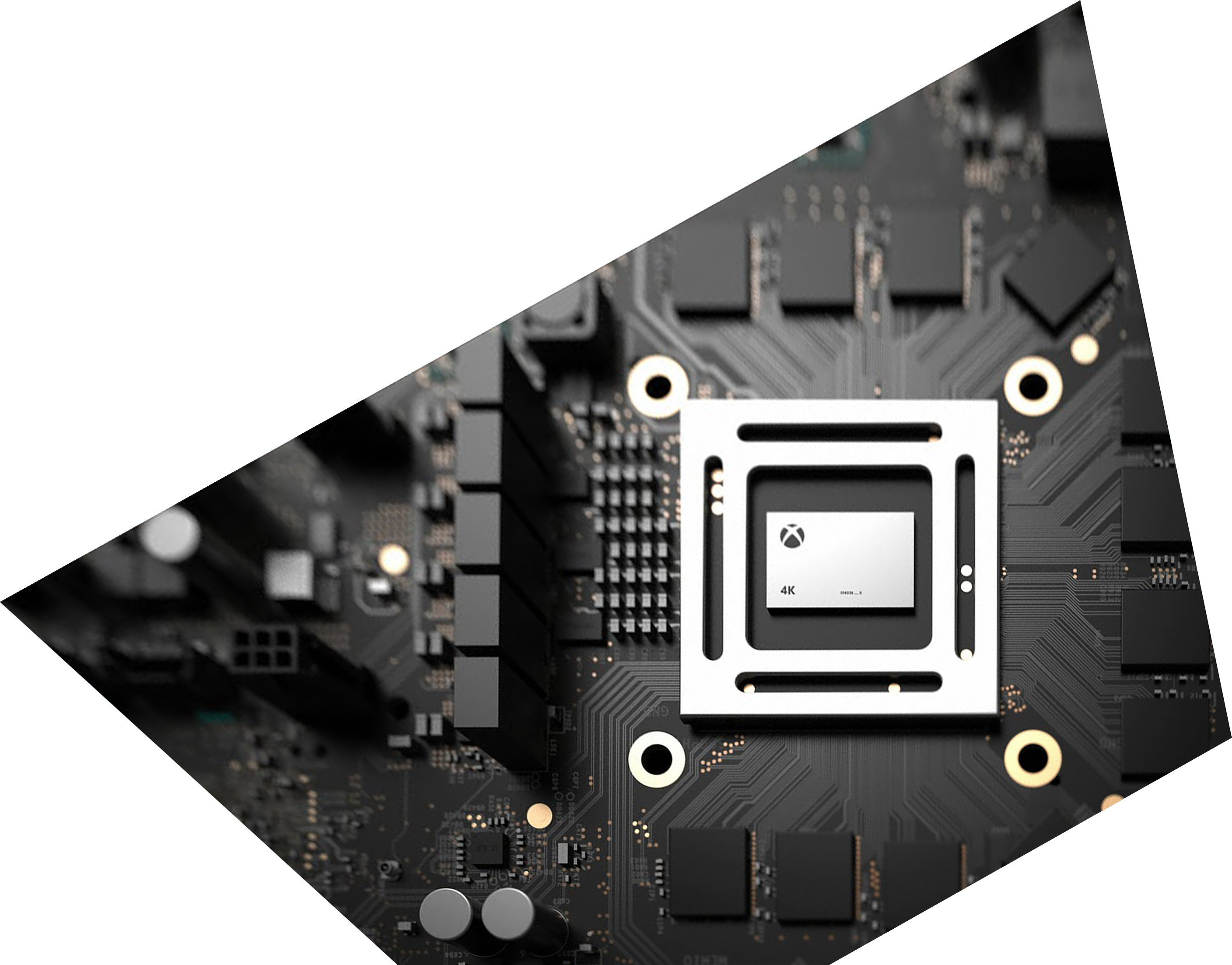
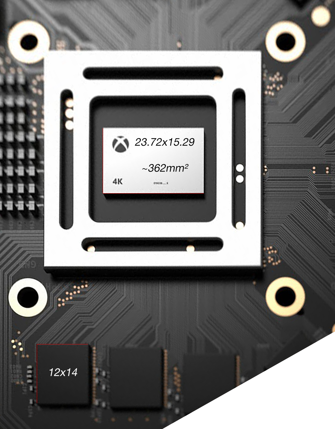
Just did some simple math, fyi a 40CU polaris (with 2560 shader cores) can reach the 6 TFLOP number if it is clocked at 1.17Ghz, which we still don't know what sort of temps and power draw it's reaching to do that (stock RX480 is running at 1.266Ghz). This seems more plausible to me rather than the Vega simply because both the CPU and GPU have to be crammed in a single soc and the bigger die usually means more heat + more space + higher power draw, three things you want to avoid when building a console.

Can we really expect a full chip to be used in consoles? I would prefer it over Vega if it means MS has enough space to put Zen in.
 
I doubt GDDR5X will be completely abandoned in the Vega lineup. HBM2 will be for their most expensive models in their lineup. The cost of HBM2 will still be quite expensive in 2017 late. Cheaper HBM1 cannot even be momentarily considered because of its 4GB memory limit.

GDDR5X currently reaches 10Gbps per pin but there JEDEC roadmap plans over the next few years to roll out 12Gbps, 14Gbps and eventually 16Gbps per pin modules.
GDDR5 for Vega will be interesting. Seems like it would come down to the size of the dies and they seem to have left a gap between Polaris 10 and small Vega. There were rumors of a 4k CU Polaris a while back that I'd have to imagine was HBM1 based just to get the bandwidth. It seems to have disappeared though. A more cost competitive option might be a single stack of HBM1/2 (maybe 1GB as opposed to 32MB ESRAM) for framebuffer/rops and DDR4 for everything else. That's the approach that was seemingly used in a research paper covering the Zen architecture a while back. Applying that Zen design to scorpio would seem logical.

This seems more plausible to me rather than the Vega simply because both the CPU and GPU have to be crammed in a single soc and the bigger die usually means more heat + more space + higher power draw, three things you want to avoid when building a console.
On the other hand it is a premium box and the SOC might be far easier to cool. A bigger chip at lower clocks would be the more power efficient design.
 
If Scorpio is a soc, why would it need to have a configuration thats the same or similar to a desktop part? There is nothing to stop them from doing a 48 CU part.
 
By the way, i just did a quick perspective crop of the official image on the xbox site if anyone wants to measure the die size, it's not perfect but it's definitely better than the angled shots they released :)

scorpiofljl3.png
 
GDDR5 for Vega will be interesting. Seems like it would come down to the size of the dies and they seem to have left a gap between Polaris 10 and small Vega. There were rumors of a 4k CU Polaris a while back that I'd have to imagine was HBM1 based just to get the bandwidth. It seems to have disappeared though. A more cost competitive option might be a single stack of HBM1/2 (maybe 1GB as opposed to 32MB ESRAM) for framebuffer/rops and DDR4 for everything else. That's the approach that was seemingly used in a research paper covering the Zen architecture a while back. Applying that Zen design to scorpio would seem logical.


On the other hand it is a premium box and the SOC might be far easier to cool. A bigger chip at lower clocks would be the more power efficient design.
Sorry my dismissal of HBM1 was regarding Scorpio, not for discreet Vega based PC videocards. Ignoring the 3d rendering of the scorpio silicon in the e3 reveal trailer, a single 8gb module of HBM1 only provides 128GBps so it wouldn't provide the bandwidth necessary memory bandwidth coupled with 256bit wide ddr4 bus @ 2.133Ghz (136 GBps) to reach the Scorpios 320GB/s they announced. Also not sure how the memory controller layout would work with 2 external forms of memory going to the same SoC.
 
The die render looks a bit smaller than the current X1 apu (363 mm²), but that wouldn't be too surprising given that it doesn't have ESRAM taking space anymore, that and the 14nm FF+ process

microsoft_xbox_one_so7ck3c.jpg
 
The die render looks a bit smaller than the current X1 apu (363 mm²), but that wouldn't be too surprising given that it doesn't have ESRAM taking space anymore, that and the 14nm FF+ process

microsoft_xbox_one_so7ck3c.jpg

Where is that from? Is that legit?
 
Where is that from? Is that legit?

https://www.ifixit.com/Teardown/Xbox+One+Teardown/19718

That's not the Xbox One S btw

Edit: Fyi Polaris 10 die is measured at 232mm²

Judging by the die size in the render i can't see how the Scorpio using Vega on top of having a CPU in the same die (although we don't know the exact size of Vega we have to assume that it's at least >= 300mm²). On the other hand, that's still a render so it might not represent the final die at all.

For reference, the 7790 (PC X1 equivalent GPU) is measured at 160mm² but then you have the ESRAM taking space in the die, that won't happen in the Scorpio.
 
Last edited:
https://www.ifixit.com/Teardown/Xbox+One+Teardown/19718

That's not the Xbox One S btw

Edit: Fyi Polaris 10 die is measured at 232mm²

Judging by the die size in the render i can't see how the Scorpio using Vega on top of having a CPU in the same die (although we don't know the exact size of Vega we have to assume that it's at least >= 300mm²). On the other hand, that's still a render so it might not represent the final die at all.

For reference, the 7790 (PC X1 equivalent GPU) is measured at 160mm² but then you have the ESRAM taking space in the die so that won't happen in the Scorpio.

Again. It's a modular design. If for example, VEGA has 60 CUs (pulling number out of my arse), there's no reason Project Scorpio couldn't have 40 CUs or 44 CUs or even 52 CUs.

Just like PlayStation Neo could have 36 CUs or 32 CUs or 28 CUs or even 40 CUs. Being based on Polaris or Vega doesn't mean you need to have the same CU count or size of Polaris 10/11 or Vega 10/11.

Regards,
SB

Yeah i agree, even if the number of CUs is final right now we won't know until they reveal some specs definitely.
 
If Scorpio is a soc, why would it need to have a configuration thats the same or similar to a desktop part? There is nothing to stop them from doing a 48 CU part.
Honestly I hope it is not a SOC, I think SOC are oversold, especially now that console have taken that giant stride to catch up with PC with regard to the amount of memory. Highest end PC card have about 4GB of VRAM to handle the resolution targeted by those new systems, why pay for twice or trice that amount of the most expensive memory type? On the other hand that bandwidth does really few for CPU so you can use relatively affordable memory for the main pool of RAM.

For reference, the 7790 (PC X1 equivalent GPU) is measured at 160mm² but then you have the eSRAM taking space in the die, that won't happen in the Scorpio.
As time passes I wonder more and more about why MSFT did not simply use it and simply designed a custom CPU. They wanted lots of RAM a NUMA design,was the best safest way to do that. It is paradoxal for a company name MSFT for which dealing with PC is every bread and butter to not see how efficient the PC take on the matter, born of practicality, has become.
 
Well we know it's 6Tflops and consoles generally have lower clock speeds so to me this thing has to have at least 52CU's.
 
Well we know it's 6Tflops and consoles generally have lower clock speeds so to me this thing has to have at least 52CU's.

Again i can't see how that is feasible with the current render. Doing some simple math, assuming a similar architecture to Ps4 apu (348 mm²)

ps4-reverse-engineerecykoi.jpg


The total die size for the GPU they modeled this after was 212mm² (Pitcairn XT). The total size taken in the complete die just for CUs is around 114mm² (for 20 GCN CUs). The Scorpio render points towards a < 363mm² die (smaller than X1) and let's assume that due to FF+ the jaguar cores (or whatever used) take less space in the new die that seems to be around ~300mm² < Scorpio < X1 363mm² and let's give an extra 20% space for the CUs that takes it up to around 140mm² which would fall in line perfectly with how Polaris 10 sees an increase in size coming from Pitcairn XT to around 232mm². That's the most "accurate" (it isn't) analysis we can deduce from the data available from current generation consoles and the pictures available from MS. 52, 56 or 60 CUs would see a great size increase in the die itself, which is not apparent in the PR render.
 
Last edited:
Again i can't see how that is feasible with the current render. Doing some simple math, assuming a similar architecture to Ps4 apu (348 mm²)

ps4-reverse-engineerecykoi.jpg


The total die size for the GPU they modeled this after was 212mm² (Pitcairn XT). The total size taken in the complete die just for CUs is around 114mm² (for 20 GCN CUs). The Scorpio render points towards a < 368mm² die (smaller than X1) and let's assume that due to FF+ the jaguar cores (or whatever used) take less space in the new die that seems to be around 300mm² < Scorpio < X1 368mm² and we'll let's give an extra 20% space for the CUs which takes it up to around 140mm² which would fall in line perfectly with how Polaris 10 sees an increase in size coming from Pitcairn XT to around 232mm². That's the most "accurate" (it isn't) analysis we can deduce from the data available from previous generation consoles and the pictures available from MS. 52, 56 or 60 CUs would see a great size increase in the die itself, which is not apparent in the PR render.
I'm not taking the renders in the Scorpio PR video literally. Microsoft wanted visuals to go along with the people talking about the system. Probably semi-accurate/half mockup.
 
Honestly I hope it is not a SOC, I think SOC are oversold, especially now that console have taken that giant stride to catch up with PC with regard to the amount of memory. Highest end PC card have about 4GB of VRAM to handle the resolution targeted by those new systems, why pay for twice or trice that amount of the most expensive memory type? On the other hand that bandwidth does really few for CPU so you can use relatively affordable memory for the main pool of RAM.
SoCs are definitely not oversold, especially in case of consoles. Having APU/SoC opposed to separate CPU and GPU opens a world of difference in heterogeneous computing
 
SoCs are definitely not oversold, especially in case of consoles. Having APU/SoC opposed to separate CPU and GPU opens a world of difference in heterogeneous computing
That is all jazz, PC are doing really well without it, actually what devs wants and is always the same more serial performances which consoles are still lacking. The tests ran by DF among others with cheap PC and the last pentium CPU are a testament to that.

A real issue with SOC is provide the system with fast enough RAM, the need for VRAM are pretty known one only has to look at shipping PC GPUs and that less than the require amount of main. You could have NUMA and SOC though no one ever tried that. I suspect that is easier to manage heat and power if you have two chips that operates in significantly different manners.
 
Last edited:
Okay, since nobody tried to do it, i did try to measure the die in the render myself, using the metrics for the memory module provided by micron (which we assume is gddr5): https://www.docdroid.net/7fus1i6/4gb-gddr5-sgram-brief.pdf.html

The final count comes up to 15.15mm height x 23.57mm width which turns out to 357mm² for the Scorpio. So let's say ± 10mm² for the sake of accuracy, the render falls between the Ps4 (348mm²) and X1 (363mm²), but in a newer process. And once again, this is my first time trying to measure a die so i don't really know how accurate that is. Although the memory modules themselves come up to 12x14 almost perfectly.
 
Last edited:
Second attempt and an image

scorpiomeasure7jjms.png


Non rounded numbers:

Height: 15.298245614035087719298245614035
Width: 23.719298245614035087719298245614
Die size: 362.86365035395506309633733456448

Actually pretty similar to X1 in terms of size if this is correct, which i'm not sure about as i'm hardly an expert in measuring dies :p

Math logic behind the measurement
  • Draw line over memory module width (which according to micron is 12mm)
  • Measure how many pixels on that line -> 12mm line = 171 pixels
  • Draw lines for width and height on the die
  • Measure pixels of each line in the actual die -> (#pixels/171)x12 = mm of each respective line on the die
  • Multiply -> Profit

Just to test, used the exact same method for this (GM200): https://www.techpowerup.com/reviews/NVIDIA/GeForce_GTX_980_Ti/images/front_full.jpg

And the total die size came up to 600.49690695619239994950132559021, reported nvidia die size is 601mm² so i guess that's pretty close :)
 
Last edited:
By the way, i just did a quick perspective crop of the official image on the xbox site if anyone wants to measure the die size, it's not perfect but it's definitely better than the angled shots they released :)

scorpiofljl3.png
Very nice and excellent/smart investigation on the chip they've shown. Thanks for sharing.

ps. I wonder if you used gimp to get the picture in perspective
 
Status
Not open for further replies.
Back
Top