AMD: Pirate Islands (R* 3** series) Speculation/Rumor Thread

http://semiengineering.com/time-to-revisit-2-5d-and-3d/

This article lays out a variety of cost and yield factors.

Along the way is the interesting metric of 25c per square mm for an interposer, about 5x the cost of DRAM.

Clearly, throwing away an entire interposer because you broke it putting the memory on there is costly. But I can't find a discussion of yield rates for completed assembly of components upon an interposer anywhere, as yet. Getting yield for individual HBM modules after mounting on the interposer seems to be a distant prospect. Assessing yield in terms of the loss of one or more channels inside an HBM module due to assembly on the interposer seems like wishful thinking.

If that was a factor then redundancy would be built into the physical spec of HBM. It may well be already. In either case, the discussion of channel loss seems fruitless, though the rummage was interesting.
 
Along the way is the interesting metric of 25c per square mm for an interposer, about 5x the cost of DRAM.
Wow, that's insanely expensive. I was reading up on this stuff yesterday and saw a target of $2 per 100mm2, which would still be $16 for a 800mm2 interposer.
 
Wow, that's insanely expensive. I was reading up on this stuff yesterday and saw a target of $2 per 100mm2, which would still be $16 for a 800mm2 interposer.

Sure, but that's from a year ago. One assumes AMD has waited until the cost has come down to something more reasonable.
 
The way the article puts it, the estimated cost of an interposer is 5x per mmm2 of cheap DRAM you can buy at the store, which HBM is not.
The following article puts HBM and HMC at a 2x multiple of LPDDR3, which is not the cheapest RAM.
http://chipdesignmag.com/display.php?articleId=5279
In the case of a GPU with 8GB of HBM on a custom logic die, that is 8 stacks with ~42mm2 each, which is an aggregate area and cost that is in the same order of magnitude as the interposer.
And one may not fully know the state of the system until the GPU is attached.

At that point, it seems straightforward to do what salvage GPU SKUs do and shut off portions if they don't work.
 
The design of the HBM could be based one the PIM work they (AMD Research) did in 2014.. We discussed this a while ago, just can't remember/find which thread it was in :)
That's an interesting (and maybe rather obvious) way to go, but how do you cool the base die? There just couldn't be much heat dissipation or it would kill itself with no direct cooling. Or overheat the DRAM die directly above it, then kill itself. ;)
 
This could be the case.
Perhaps someone more familiar with the shorthand for DRAM signal assignments than I can point to which labels would be redundant command and data IOs on page 20 of the following.
http://www.cs.utah.edu/thememoryforum/mike.pdf
Interesting PDF. At 20 pJ/bit, a 336 GB/s interface takes about 54 Watts. At 7 pJ/bit, a 640 GB/s interface takes 19 W. So the power savings we'd expect for the rumored Fiji interface over Titan is around 30 W.
 
That's an interesting (and maybe rather obvious) way to go, but how do you cool the base die? There just couldn't be much heat dissipation or it would kill itself with no direct cooling. Or overheat the DRAM die directly above it, then kill itself. ;)
The general case answer is that the logic layer is capped in its power consumption. The previously mentioned paper on this assumed a 10W TDP, which was high enough to give the design something to do, but low enough that temperatures did not exceed 85C and cause performance loss in the DRAM due to excessive refreshes. This means that the workloads need to be evaluated in terms of how much they benefit from the ready bandwidth versus how much peak performance is lost due to hardware that is very limited by dissipation concerns. Area available for compute is somewhat limited as well, since this is a small-footprint device and it needs to serve as a DRAM as well.
http://www.dongpingzhang.com/wordpress/wp-content/uploads/2012/04/TOP-PIM-HPDC-paper.pdf

Interesting PDF. At 20 pJ/bit, a 336 GB/s interface takes about 54 Watts. At 7 pJ/bit, a 640 GB/s interface takes 19 W. So the power savings we'd expect for the rumored Fiji interface over Titan is around 30 W.
This is sort of around where it was guessed that a GPU memory interface at 25-30% of 300 TDP with 40-50% power savings would save.
 
Interesting PDF. At 20 pJ/bit, a 336 GB/s interface takes about 54 Watts. At 7 pJ/bit, a 640 GB/s interface takes 19 W. So the power savings we'd expect for the rumored Fiji interface over Titan is around 30 W.
Actually, 19W should be 336GB/s on HBM, while 640GB/s is 36W with the quoted consumption at least.
 
This could be the case.
Perhaps someone more familiar with the shorthand for DRAM signal assignments than I can point to which labels would be redundant command and data IOs on page 20 of the following.
http://www.cs.utah.edu/thememoryforum/mike.pdf
That diagram is showing the intra-stack TSV organisation, as far as I can tell. Which is part of what's defined in the HBM standard. Enabling third parties to create their own base die, which can inter-operate with multiple vendors' DRAM stacks.

If we're talking about failure modes during assembly of a module to an interposer, then the physical interface from the base die to the ASIC is entirely within the ASIC supplier's control. Which is precisely where I would expect redundancy to apply (if this failure mode is significant). The cost per trace in the ASIC-interposer-base die is obviously relatively low, so ~13% extra traces is practical.

This paper on Citadel, an alternative to ECC, which is a couple of percent more costly in terms of area, is pretty interesting:

www.cs.utah.edu/thememoryforum/nair.pdf

This paper proposes Citadel, a robust memory architecture that allows the memory system to store each cache line entirely within one bank, allowing high performance, low power and efficient protection from large-granularity failures. Citadel consists of three components; TSV-Swap, which can tolerate both faulty data-TSVs and faulty address-TSVs; Three Dimensional Parity (3DP), which can tolerate column failures, row failures, and bank failures; and Dynamic Dual-Granularity Sparing (DDS), which can mitigate permanent faults by dynamically replacing faulty memory regions with spares, either at a row granularity or at a bank granularity. Our evaluations with real-world DRAM failure data show that Citadel performs within 1% of, and uses only an additional 4% power versus a memory system optimized for performance and power, yet provides reliability that is 7x-700x higher than symbol-based ECC.

The references section looks useful.

Clearly the topic of intra-stack TSV redundancy exists (though I can't discern whether it's present in the NVidia slide deck). I still haven't found a discussion of interposer-to-device redundancy.
 
That's an interesting (and maybe rather obvious) way to go, but how do you cool the base die? There just couldn't be much heat dissipation or it would kill itself with no direct cooling. Or overheat the DRAM die directly above it, then kill itself. ;)

As others have said there would be a TDP limit on it but there are extra TSVs added that allow for even thermal distribution so heat doesn't get trapped in the stack.
Edit- Correction, not TSVs but "Thermal Dummy Bumps"

Source


ThruChip Wireless is awesome:

http://www.hotchips.org/wp-content/...Kuroda_Lee.-ThruChip-v24_final_submission.pdf

The manufacturability is super-easy, with the presumption that ultra-thinning of wafers (< 10μm) gets wide adoption.

We're talking a factor of 10 improvement in power.
Wow, that is some amazing stuff.
 
Last edited:
ThruChip Wireless is awesome:

http://www.hotchips.org/wp-content/...Kuroda_Lee.-ThruChip-v24_final_submission.pdf

The manufacturability is super-easy, with the presumption that ultra-thinning of wafers (< 10μm) gets wide adoption.

We're talking a factor of 10 improvement in power.

That is an impressively thin wafer thickness if it can be done at a mass scale, and the comparison with the high aspect ratio of TSVs is interesting.
I'm curious if the possibility exists for TSVs with a low aspect enabled by this level of thinning.

That very thin wafer thickness and discussion of highly-doped silicon for power delivery also brought to mind IBM's eDRAM process. With that level of thinning, it would be possible to grind the bottom of a die with eDRAM to the point that the trenches could be interfaced from the top and bottom, or any other sort of shenanigans one could dream up with highly-regular silicon structures with whatever compounds and voltages could be injected into those interfaces.
 
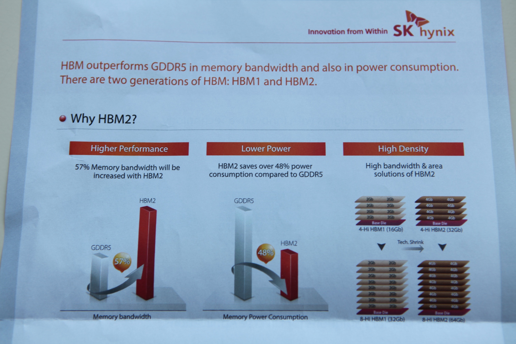
As Hynix appears to stack four or eight 4Gbit dies in their first HBM generation before they go to 8Gbit per die with a process shrink in their second generation of products, all this dual-link stuff could be the result of a fake. If Hynix indeed offers stacking of 4Gbit dies (the versions with 2Gbit dies being more of a test run?), Fiji is likely getting just four 4Hi stacks of these with a capacity of 2 GB per stack.

gtc2015-skhynix-2.jpg
 
As Hynix appears to stack four or eight 4Gbit dies in their first HBM generation before they go to 8Gbit per die with a process shrink in their second generation of products, all this dual-link stuff could be the result of a fake. If Hynix indeed offers stacking of 4Gbit dies (the versions with 2Gbit dies being more of a test run?), Fiji is likely getting just four 4Hi stacks of these with a capacity of 2 GB per stack.
All the HBM1's have 2Gbit dies there, but it does show new things - it shows exactly what the leaked AMD slides show too, "dual-link" 16Gbit per 4-Hi stack with 4 layers of 2x2Gbit DRAMs instead of 1x2Gbit? The 8-Hi shouldn't be happening on HBM1's though, it was supposed to come with HBM2 too.
 
Last edited:
Has Hynix (or anyone else, for that matter) said anything about the power consumption of HBM2 vs. HBM1?
 
All the HBM1's have 2Gbit dies there, but it does show new things - it shows exactly what the leaked AMD slides show too, "dual-link" 16Gbit per 4-Hi stack with 4 layers of 2x2Gbit DRAMs instead of 1x2Gbit? The 8-Hi shouldn't be happening on HBM1's though, it was supposed to come with HBM2 too.
I would say it shows 2 Gbit per channel (with 2 channels on a die), so 4Gbit dies, no "dual-link". And the factor 2 in density for a process shrink between HBM1 and HBM2 (using 8Gbit dies) appears reasonable, too. But Hynix material often contains errors, maybe one shouldn't place too much faith in details. The take home message is probably that Hynix offers (or will offer) 16 Gbit and even 32Gbit HBM1 stacks without the need for custom logic dies or some other tinkering with the HBM standard.
 
Back
Top