
FWIW I only get 12GB/sec pver PCIe with NVIDIA's BandwidthTest tool. Versus the 512MB segment, which comes close to that 28GB/sec number, it's a pretty big difference even before taking latency into account.Reading from last 512mb vram in gtx970 is 22GB/s, and pci express 3 is 16GB/s so no big difference, but to read from system ram we have to copy it to vram(16GB/s) and then read from vram, thats the difference ?
You are using an out of date browser. It may not display this or other websites correctly.
You should upgrade or use an alternative browser.
You should upgrade or use an alternative browser.
That might depend on how much remains before hitting a synchronization point in the renderer, or some kind of broad dependence on the data being requested.
The memory bus delay is ~1KB of data not transfered for one cycle.
The PCIe transfer involves hoping the GPU will find something to do for microseconds.
It's still better than some early studies on immature GPU compute where it could go for hundreds or thousands of microseconds.
The memory bus delay is ~1KB of data not transfered for one cycle.
The PCIe transfer involves hoping the GPU will find something to do for microseconds.
It's still better than some early studies on immature GPU compute where it could go for hundreds or thousands of microseconds.
It seems like the diagram is still a lie
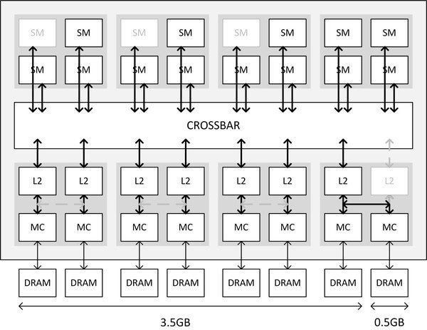
The 'crossbar' diagram from Anandtech and other places speaking on behalf of Nvidia is STILL a LIE. Let me explain why.
If the so-called memory block diagram were true (and this design was assumed by sites like Anandtech when the 970 was released), there'd be no reason why crippling 3/16 shader blocks would need to impact anything on the memory controller side (after all, AMD has used a cross-bar system forever, but the crippled 290 is NOT crippled at the point of memory bus access, and sees 512-bits and 4GB).
The diagrams Nvidia releases are ABSTRACTIONS that try to cast the new Maxwell architecture in terms of systems that only apply to earlier Nvidia designs.
The 970 is firstly, like the 290, a 4-way design. This means the 290 and 970 are actually internally equivalent to FOUR independent graphics cards (and the reason DX12 is so important- it allows game code to control each of the four independent systems explicitly, so one out of four, for instance, could be permanently running 'physics' code'). Then the 980/970 is also comprised of 16 shader machines (four per independent GPU block).
Each shader machine is DIRECTLY attached to a memory access block that DIRECTLY attaches to 1/16 of the real bus, and thus 1/16 of the 4GB VRAM. There is no crossbar operating here. When a shader machine is switched off (the 970 deactivates 3/16) the attached memory access block is also gone. For DATA INPUT to the chip, this is the same as losing that proportion of the bus AND VRAM. .
The so-called 'crossbar' (which isn't) actually refers to the method by which shader machine units can SHARE memory. The GPU will only work at full speed when memory usage is EXCLUSIVE (same as a multi-core CPU), but frequently code (including explicit or implicit GPU instructions) will have multiple units attempting to read the same memory addresses at the same time (like when the same texture is in use by different shader units).
There are MANY strategies to handle multiple access to the same memory, and the methods used by AMD and Nvidia are actually INDUSTRIAL SECRETS. The block diagrams shown in slides by either company do NOT describe how this really happens. One method is to NOT share memory at all, but to serialise all requests for the same memory locations on the same shader machine. At the moment (per-DX12) this is something the BLACK BOX DX11 driver must figure out.
The texture management units do have their own small caches, so in read-only situations, the SAME texture data can exist in multiple TMU blocks at the same time, but TMU cache misses will trigger the problem again.
My guess is that Nvidia attempts to ensure unique resources live in each of the 1GB VRAM blocks seen by each of the four independent render machines in the 980/970. For a texture set that exceeds 1GB in current play (ie needed for a single frame), this would represent some interesting juggling by the driver. The four shader machines in the same render machine will have better access to each others real VRAM address space.
Again, DX12 is so important because the juggling required to get the best out of GCN and Maxwell is growing increasing complex, and ONLY the game designers KNOW the best way to juggle GPU resources for their game. Memory sharing = VERY SLOW GPU function. Exclusive resources = FAST AS YOU CAN GET. But exclusive resources are a pain in the backside (and very hard to scale across GPUs with different numbers of render and shader machines). How, for instance, do you port game code optimised for a 4-way design like the 290/970 to a 2-way design like the 280/770?
We should perhaps take a moment to recall how bad games coded for FOUR CPU cores (like GTA4 and Saints Row 2) ran on dual-core CPUs. The new consoles are 6+ (weak) true cores. No sane person would build a gaming rig for AAA ports with less than 4 CPU cores. I'm pretty sure the PS4 is also a 4-way GPU (ironic, given the faster 260X chip is only 1-way). I think even the slow GPU of the Xbone may be 4-way.
Independently controllable GPU render machines are the future, just as we expect independently programmable 4+ CPU cores in our PCs. And your CPU runs a LOT faster when each CPU thread uses exclusive memory address blocks that do not overlap with other cores (unless it is a dreadful AMD Bulldozer design- snooping slows AMD caches even when memory use is exclusive). DX12 is NOT about command queue overhead (although it does fix that as a side-effect).
The 'crossbar' diagram from Anandtech and other places speaking on behalf of Nvidia is STILL a LIE. Let me explain why.
If the so-called memory block diagram were true (and this design was assumed by sites like Anandtech when the 970 was released), there'd be no reason why crippling 3/16 shader blocks would need to impact anything on the memory controller side
It's not clear to me that it does. Is see no evidence that the decision to disable ROPs and L2 slices has anything to do with the number of SMs, apart from marketing concerns (segmentation, pricing, etc.) and usefulness.
According to Damien, "[o]n both Kepler and Maxwell each SM appears to use a 128-bit datapath to transfer pixels color data to the ROPs " which means that for a given number of SMs, having more than a given number of ROPs may be pointless, but that doesn't imply that the crossbar is a lie. (The cake, however, might be.)
http://techreport.com/blog/27143/here-another-reason-the-geforce-gtx-970-is-slower-than-the-gtx-980
How do you figure that actually? 1/16 of 4GB memory would mean that each SMM can only operate within 256MB or half a memory chip. That would imply some serious amounts of talking across some magic fabric that is not a crossbar. There's also a GTX 980M which has 12 SMM and has complete bus and full 2MB L2 and all 64 ROPs.Each shader machine is DIRECTLY attached to a memory access block that DIRECTLY attaches to 1/16 of the real bus, and thus 1/16 of the 4GB VRAM. There is no crossbar operating here. When a shader machine is switched off (the 970 deactivates 3/16) the attached memory access block is also gone. For DATA INPUT to the chip, this is the same as losing that proportion of the bus AND VRAM. .
It seems like the diagram is still a lie
Do you have a link (URL) to where these comments originated since they mention make reference to block diagrams from both AMD and Nvidia?
There are MANY strategies to handle multiple access to the same memory, and the methods used by AMD and Nvidia are actually INDUSTRIAL SECRETS. The block diagrams shown in slides by either company do NOT describe how this really happens. One method is to NOT share memory at all, but to serialise all requests for the same memory locations on the same shader machine. At the moment (per-DX12) this is something the BLACK BOX DX11 driver must figure out.
I believe this is it? A comment deep in the bowels of WCCF: http://wccftech.com/nvidia-geforce-gtx-970-memory-issue-fully-explained/#comment-1818384810Do you have a link (URL) to where these comments originated since they mention make reference to block diagrams from both AMD and Nvidia?
To anyone who's now dissapointed to be owning a 970 because of this and is considering swapping it out for a better GPU - I'll buy it off you for half price! 
It wouldn't make much sense to couple the SMs to the memory subsystem without a crossbar. If only because it would be quite detrimental to the ability to recover non-perfect dies.
There are probably plenty of performance reasons as well. (e.g. how could you ever balance memory traffic among different controllers without one?)
There are probably plenty of performance reasons as well. (e.g. how could you ever balance memory traffic among different controllers without one?)
I believe this is it? A comment deep in the bowels of WCCF: http://wccftech.com/nvidia-geforce-gtx-970-memory-issue-fully-explained/#comment-1818384810
Yep, it is that, does it make sense what he says?
Moreover, is also the 970m being affected in any way?
No, it makes no sense.Yep, it is that, does it make sense what he says?
It wouldn't make much sense to couple the SMs to the memory subsystem without a crossbar. If only because it would be quite detrimental to the ability to recover non-perfect dies.
There are probably plenty of performance reasons as well. (e.g. how could you ever balance memory traffic among different controllers without one?)
The proposed scheme also appears to have the side effect of physically capping the amount of memory a program can ever address to several hundred megabytes, despite everything else in the hardware and software model allowing for general access. This seems like it would be quickly exposed as a problem.
I was thinking of a workgroup of 32 items being tasked with writing 500MB of data. It has to reside on an SM, so what does it do, pretend to write it and hope the program (or any other program) reads it?
The message also seems to read far too much into the grayed out SMs in the diagram. It was never claimed that their being disabled was the reason for the memory allocation issue, and there looks to be a misunderstanding of how the L2s work as the GPU last level cache.
Yep, it is that, does it make sense what he says?
Moreover, is also the 970m being affected in any way?
I will not see why the 970M could be affected: it has the memory controllers disabled ( 192bit bus ),
The "problem" seems more related on the crossbar > L2 > MC relation, than on the SM number disabled themselves.
But maybe someone can enlight me why they have not just finally disable the last MC + the last 0.5GB.. why have try complicate this ? ( and end simply with 224bit / 3.5GB )
Last edited:
A1xLLcqAgt0qc2RyMz0y
Veteran
But maybe someone can enlight me why they have not just finally disable the last MC + the last 0.5GB.. why have try complicate this ? ( and end simply with 224bit / 3.5GB )
Meanwhile the memory controllers are still tied together, and disabling one of them requires disabling the entire partition.
http://www.anandtech.com/show/8935/...cting-the-specs-exploring-memory-allocation/2
As described the memory controllers are paired together and you cannot disable only one of them. Your example would result in 192bit / 3.0GB.
I wonder. Apparently in "normal" operation each 32bit channel has its own L2 (and ROP), with its own crossbar connection. And striping can be done over 7 such channels obviously. So it's not quite obvious why actually 2 32bit channels must be paired together to make a 64bit MC.As described the memory controllers are paired together and you cannot disable only one of them. Your example would result in 192bit / 3.0GB.
(FWIW I think such a 224bit / 3.5GB configuration would make a lot of sense, much more so than the current GTX 970 - obviously would be a bit cheaper, with no real downside except of course now you really have a bit less memory, but on the upside it gets simpler to manage in the driver too.)
As described the memory controllers are paired together and you cannot disable only one of them. Your example would result in 192bit / 3.0GB.
So it will end like the 970M, with a 192bit bus, But they have try go higher by add this link.. and finally, today, they can enable fully the 224bit bus / 3.5GB memory.. so why not have just keep that ? why try sold us they could maybe try use in some case the 32bit left and the 0.5GB left ? ..
If we compare the situation with the mobile scenario :
- 970M = 10SM / 192bit / 3GB ( 2.5 GPC )
- 980M = 12SM / 256bit / 4GB ( 3 GPC )
- G970 = 13SM / 224bit / 3.5GB ( + 32bit slow, 0.5GB ) ( 3.25 GPC ? )..
- G980 = 16SM / 256bit / 4GB ( 4 GPC )
For me, Nvidia have work for been able to keep 224bit / 3.5GB on the 970... .. and this was allready good, the problem is the communication. they should have advertize it like that instead of play this game.
Last edited:
firstminion
Newcomer
What I meant is that you had just mentioned that in this topic.Remembered? That information came from NVIDIA (Jonah) back on Sunday.
Babel-17
Veteran
http://www.anandtech.com/show/6159/the-geforce-gtx-660-ti-review/2
Is that relevant to this, in that nVidia had this option but chose otherwise? I feel like I should stay out of this conversation, it's way (way) over my head, but I'm curious as to why the the story of the 660-Ti gets no mention. Does it have no bearing?
Is that relevant to this, in that nVidia had this option but chose otherwise? I feel like I should stay out of this conversation, it's way (way) over my head, but I'm curious as to why the the story of the 660-Ti gets no mention. Does it have no bearing?
Similar threads
- Replies
- 351
- Views
- 36K
- Replies
- 121
- Views
- 15K
- Replies
- 168
- Views
- 33K