
Isn't GM204 4 FP64 per SMM, not 1? (aka 1/32 DP rate)The problem today is rumor point something like they basically will not add more FP64 units compared to GM204 ( 1 FP 64 unit / SMM ).. I will maybe bet for an 1/8 DP rate anyway ...
AMD dont use additional FP units ( well they use aditional hardware and scalar units ) but there FP32 units is able to do the FP64 one.. I dont understand why nvidia dont go this road instead of use aditional units for it.
You are using an out of date browser. It may not display this or other websites correctly.
You should upgrade or use an alternative browser.
You should upgrade or use an alternative browser.
Whoa! I wonder if it has anything to do with the introduction of the GK210? I'm not sure why the GK210 would be introduced at all if it would be succeeded by GM200 around half a year later.
Yes, but the elephant in the room is GK210. Why do it if you would have a great GM200 coming in?
They might have been constrained by 28nm to the point the increase in DP computing power would be less than what would be possible with an optimised Kepler core (GK210) in a dual chip card. They could have compared the numbers in advance and since Kepler is already a mature architecture, it could have made more sense and safe to do that, rather than pushing for a larger GM200 chip on a new architecture.
Let me first start off by saying I believe GM200 is DP heavy, whether 1:4 or 1:2 or any other number I dont know..but I certainly believe that the DP rate is significantly higher than GM204.
Now regarding why release GK210 if GM200 is to follow? Well one thing to remember is that GK210 is late..IIRC it was supposed to release by mid 2014...or maybe even earlier. Sot it should have had a decent window to sell before GM200 came out. GM200 has yet to release and typically we see that the professional parts lag the consumer parts by ~6 months. So it should have had about a year's window or more to sell. Even with the delay..since it was ready and the cost already sunk..why not release it anyway and recover as much money as you can until GM200 comes out?
Oh I dont get another thing about GK210. Its meant to be compute focused so why not strip it down further of even excess ROPs and TMUs..those dont really have any bearing on compute performance. There would have been available die area to further increase SP and/or DP performance. Since they designed a whole new die, wouldn't this have been feasible?
Damn, that's a crapload of ROPs, if not a fake... Would a GPU be able to utilize that many though with less than 320GB/s available to it? Caching framebuffer pixels in L2 would help, but would it be enough to make the chip efficient?
Thats the exact question I've asked already and I'm still not convinced its necessary. 2x the ROPs of GK110 seems a bit overkill. And the clocks are higher this gen too so fillrates are higher anyway.
I believe the same question was asked about GM204 and we all know the results there. I think the key lies in the increased L2 amount relative to Kepler, as well as the delta color compression technology. Also, 320GB/s is a ton of bandwidth.
About GM204's performance..if you look at it from another angle..GTX 980 has about 70% more fillrate than GTX 780 Ti..but only about 10% more performance (Combination of 33% more ROPs and 30% higher clocks). So is that really efficient?
Didn't NVIDIA rep already say that they're skipping compute on Maxwell and there won't be "real DP part"?Let me first start off by saying I believe GM200 is DP heavy, whether 1:4 or 1:2 or any other number I dont know..but I certainly believe that the DP rate is significantly higher than GM204.
iMacmatician
Regular
The GK210 being late definitely puts matters in perspective. I'm not convinced that the professional/consumer trend holds anymore (for NVIDIA) after the GK110. IIRC the GK180/GK110B was also professional first.Now regarding why release GK210 if GM200 is to follow? Well one thing to remember is that GK210 is late..IIRC it was supposed to release by mid 2014...or maybe even earlier. Sot it should have had a decent window to sell before GM200 came out. GM200 has yet to release and typically we see that the professional parts lag the consumer parts by ~6 months. So it should have had about a year's window or more to sell. Even with the delay..since it was ready and the cost already sunk..why not release it anyway and recover as much money as you can until GM200 comes out?
Perhaps the original intention was to use GK210 in the GeForce and/or Quadro lines as well, but those plans got shelved after the GK210 delay. (That assumes, of course, that the GK210 won't be used in any future products in those lines.) However, if the GM200 has slow DP then there's still a place for a GK210-based GeForce TITAN, regardless of any delays.Oh I dont get another thing about GK210. Its meant to be compute focused so why not strip it down further of even excess ROPs and TMUs..those dont really have any bearing on compute performance. There would have been available die area to further increase SP and/or DP performance. Since they designed a whole new die, wouldn't this have been feasible?
I'm not knowledgeable enough to actually answer this question, but here's my thought regarding that angle: A GM204 with half the ROPs removed running at the same clocks as the 980 would have lower performance than the 980. What would happen if the GM204 with 32 ROPs were scaled up and/or clocked higher to match the 980 in overall performance while keeping the ROP count?About GM204's performance..if you look at it from another angle..GTX 980 has about 70% more fillrate than GTX 780 Ti..but only about 10% more performance (Combination of 33% more ROPs and 30% higher clocks). So is that really efficient?
Game-debate has some possible specs of big maxwell!
What do the esteemed knowledgeable members of B3D think?
Any validity, or click bait thin air?
At first glance the pixel fillrate already seems wrong for 96rops, if I am not mistaken.
What do the esteemed knowledgeable members of B3D think?
Any validity, or click bait thin air?
At first glance the pixel fillrate already seems wrong for 96rops, if I am not mistaken.
Clickbait, as are most "rumors" of this type. Just my opinion, of course.
Game-debate has some possible specs of big maxwell!
What do the esteemed knowledgeable members of B3D think?
Any validity, or click bait thin air?
At first glance the pixel fillrate already seems wrong for 96rops, if I am not mistaken.
If we look at the rumored specification of the Quadro full GM200: 384bit bus / 12GB - 3072 SP. http://www.guru3d.com/news-story/nvidia-gm200gm210-gpu-specs-surface.html
- The memory size seems wrong on GD: 8GB for a 384bit bus, 6GB seems more plausible.
- Core count wise, they seems think 1 GPC is removed ( 5GPC ).. seems plausible. ( or multiple SMM / GPC ? ).
Like allways, i got the feeling they update their " spec " based on any rumor. personally untill i see some more things, i will not touch to much of the rumor.
The tex rate and TMUs would be wrong, it'd have 16:1 shaders:TMUs, so 160 TMUs not 150. 2560 shaders also seems quite low for large Maxwell, would Nvidia "only" have a 25% increase over GM204?
The full Maxwell is rumored to be 3072SP for 6GPC . i suppose they had remove 1 GPC ( 512SP ) for this equation.. This said.. impossible to know.
Ah I see.
So 5GPCs, means 80rops, 160tmus, 2560cores, 384bit ram, 6BG video ram?
Somethink like that?
So we are expecting 1/4 more performance than the 980 in essence?
Personally i will more count on the 3072SP version for the TI but... well hard to know, as maybe the 3072SP are completely wrong.
Didn't NVIDIA rep already say that they're skipping compute on Maxwell and there won't be "real DP part"?
Really? I must have missed it if they did. Any source or link for this?
The GK210 being late definitely puts matters in perspective. I'm not convinced that the professional/consumer trend holds anymore (for NVIDIA) after the GK110. IIRC the GK180/GK110B was also professional first.
Thats true to a certain extent..I do think they have concentrated heavily on professional over the last few years. But my point is that the professional parts always come out after the consumer parts due to the extra validation/testing/certification required of both the hardware and software. I dont know much about GK110 so not sure about where it was first seen.
Perhaps the original intention was to use GK210 in the GeForce and/or Quadro lines as well, but those plans got shelved after the GK210 delay. (That assumes, of course, that the GK210 won't be used in any future products in those lines.) However, if the GM200 has slow DP then there's still a place for a GK210-based GeForce TITAN, regardless of any delays.
I don't see much utility in using GK210 in the Geforce line. Given the timing of GM204, this would have made no sense. Quadro maybe. Yep..if the GM200 does have slow DP, then GK210 will still have a place in segments which require DP performance. However, GM200 will absolutely slaughter it in SP performance (especially performance/watt).
I'm not knowledgeable enough to actually answer this question, but here's my thought regarding that angle: A GM204 with half the ROPs removed running at the same clocks as the 980 would have lower performance than the 980. What would happen if the GM204 with 32 ROPs were scaled up and/or clocked higher to match the 980 in overall performance while keeping the ROP count?
Well I am not saying they should have stayed at 32 ROPs. Maybe something in between would have been more area efficient, say 12 ROPs per MC so 48 ROPs for GM204 and 72 for GM200. However, given the usual power of 2 configs they like to use (i.e. 4, 8 or 16 ROPs per MC), I am not sure if this would have been feasible either. And as others have stated, always better to have more fillrate than less! And about your question, I guess noone outside of Nvidia actually could answer it!
Ah I see.
So 5GPCs, means 80rops, 160tmus, 2560cores, 384bit ram, 6BG video ram?
Somethink like that?
So we are expecting 1/4 more performance than the 980 in essence?
ROPs would be 96, they dont scale with GPCs but with the MCs. 384 bit would be 96 ROPs.
With 5 GPCs, yes I believe 20-25% would be a reasonable expection. But the full 6 GPC config should be 40% or more.
iMacmatician
Regular
From Videocardz: "Exclusive: NVIDIA Maxwell GM206 pictured."
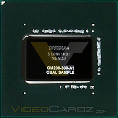
Can anyone give a good estimate of the die size from this picture? I normally use the background dots to scale these pictures but I can't see them in this one. The small triangle on the upper left corner seems too small. The only other thing I can think of is to use the four white points on the diagonals, but the locations of them vary depending on the chip.
Also, from the link, the specs of the 960 are as follows: 1178 MHz core clock, 2 GB 128-bit GDDR5, 7010 Mbps.
GK110 introductions:Thats true to a certain extent..I do think they have concentrated heavily on professional over the last few years. But my point is that the professional parts always come out after the consumer parts due to the extra validation/testing/certification required of both the hardware and software. I dont know much about GK110 so not sure about where it was first seen.
- Tesla K20, K20X: November 2012
- GeForce GTX TITAN: February 2013
- GeForce GTX 780: May 2013
Something could obviously be lost in translation butReally? I must have missed it if they did. Any source or link for this?
https://translate.google.com/translate?hl=en&sl=ja&tl=en&u=http://www.4gamer.net/games/121/G012181/20141225075/
By the way, the current Tesla has continued to use the architecture of the "Kepler" generation, but I wonder if there is that these are switched to Maxwell.
Mr. Lin about this, was clearly deny the possibility. Says, "Maxwell will not be used in such a way of Tesla because there is no double-precision (floating-point unit). (Then) the double precision enters becomes to Pascal" and things. This means that of 2015 NVIDIA, although promote the transition to Maxwell in the graphics field, but not so that will continue to expand the Kepler in the HPC field.
For those who can read Japanese http://www.4gamer.net/games/121/G012181/20141225075/
ところで,現在のTeslaは「Kepler」世代のアーキテクチャを利用し続けているが,これらがMaxwellに切り替わることはあるのだろうか。
これについて林氏は,明快にその可能性を否定した。 曰く,「Maxwellは倍精度(浮動小数点演算ユニット)がないのでTeslaのような形で使われることはない。(次に)倍精度が入るのはPascalになる」とのこと。 つまり2015年のNVIDIAは,グラフィックス分野ではMaxwellへの移行を進めるものの,HPC分野では引き続きKeplerを展開していくことになるわけだ。
From Videocardz: "Exclusive: NVIDIA Maxwell GM206 pictured."
Can anyone give a good estimate of the die size from this picture? I normally use the background dots to scale these pictures but I can't see them in this one. The small triangle on the upper left corner seems too small. The only other thing I can think of is to use the four white points on the diagonals, but the locations of them vary depending on the chip.
Also, from the link, the specs of the 960 are as follows: 1178 MHz core clock, 2 GB 128-bit GDDR5, 7010 Mbps.
Its a bit difficult to estimate since its very fuzzy. I did a quick comparison to a GM204 die shot and tried to line up and scale according to the position of the triangle. From my very rough estimation its about ~70% of the die size of GM204 so ~ 280 mm2.
I then also did a comparison with a die shot of GK106 and it appears to be about 20% larger than GK106 so around ~260 mm2 in that case. Bear in mind this was very rough so I could be off by a decent amount in both the analyses. However, I was expecting it to stay under 250 mm2 so it does seem a bit large..almost as big as GK104 if we take the high end of my range. I would expect 10 SMMs if this were the case.
Oh and I would be surprised if it was only 128 bit..I was expecting 192 bit and 3 GB GDDR5 as the standard configuration.
Oops that was meant to read GK110B. I was responding to your point that GK110B first came out in the professional segment and replied that I wasn't sure if it did.GK110 introductions:
- Tesla K20, K20X: November 2012
- GeForce GTX TITAN: February 2013
- GeForce GTX 780: May 2013
Something could obviously be lost in translation but
https://translate.google.com/translate?hl=en&sl=ja&tl=en&u=http://www.4gamer.net/games/121/G012181/20141225075/
For those who can read Japanese http://www.4gamer.net/games/121/G012181/20141225075/
Thanks..that is a bit telling. However, just to nitpick a bit..since GM200 wasn't out when he made those statements..perhaps be was talking about GM204?
Last edited:
iMacmatician
Regular
Oh, I see (I should have looked at the context more). As far as I know, the GK110B was first introduced in the Quadro K6000 in July 2013, then in the GeForce 780 Ti and Tesla K40 in November 2013 (the 780 Ti was announced a bit earlier). I'm not sure when the cards actually started shipping though.Oops that was meant to read GK110B. I was responding to your point that GK110B first came out in the professional segment and replied that I wasn't sure if it did.
Obviously possible, but then why mention "going this generation with Kepler 'till Pascal comes"?Thanks..that is a bit telling. However, just to nitpick a bit..since GM200 wasn't out when he made those statements..perhaps be was talking about GM204?
Obviously possible, but then why mention "going this generation with Kepler 'till Pascal comes"?
I used Google translate link you shared and I didn't see that exact line anywhere in the article. The only relevant quote appears to be the one you already posted. Anyways..like I said..I was just nitpicking a bit.
By the way, the current Tesla has continued to use the architecture of the "Kepler" generation, but I wonder if there is that these are switched to Maxwell.
Mr. Lin about this, was clearly deny the possibility. Says, "Maxwell will not be used in such a way of Tesla because there is no double-precision (floating-point unit). (Then) the double precision enters becomes to Pascal" and things. This means that of 2015 NVIDIA, although promote the transition to Maxwell in the graphics field, but not so that will continue to expand the Kepler in the HPC field.
PS: Anyone else had a stab at the die shot?
Would it make sense for NVidia to continue to support the new 2-wide fp16 SIMD FMAD feature to future desktop parts? Or is fp16 really most useful for mobile where you need to push a lot of pixels in comparison to the GPU size? Of course we won't know NVidia's rationale, but if fp16 were useful on the desktop, you would expect NVidia would have supported it long ago. Kepler's integer SIMD instructions seemed useful, but NVidia found otherwise and quietly removed them from Maxwell. So maybe they've found it's better to keep the ISA as clean as possible.
Similar threads
- Replies
- 351
- Views
- 36K
- Replies
- 121
- Views
- 15K
- Replies
- 168
- Views
- 32K