AMD: Pirate Islands (R* 3** series) Speculation/Rumor Thread

Interesting recent AMD

hmmm PS Vita has a curious multilayer chip on interposer, there are some nice pics around about that.
Still, I think the layers communicate on the border there, and not with a vertical bus.
Anyway, that should be possible to add, I suppose.
 
The Vita has a single layer of Wide IO memory on top of the chip, they are bonded face to face.
The Vita package does have additional stacking, but this is less interesting because there's no direct connection between die layers, just wires that stretch down to where a conventional connection would be made.

The AMD paper shows them considering a similar to Micron's HMC, just with its own particular logic layer.
I'm not sure if this will have bearing on Pirate Islands, though, give the likely time frame from idea to execution if AMD opts to do it at all.
There are also papers or patents from AMD dealing with having secondary logic chips close to memory that perform atomics and other computation at the request of the main processors, so this can fit with that.
I see the practical need to have the compute below the DRAM stack, although it does insulate the logic from the heatsink above.

There's a hint of another HMC feature with the inter-PIM bus, which would allow different stacks to talk to each other. HMC makes provision for that as well. Another possibility, if AMD got cute with it, would be to have a generic mesh bus with connections on all four sides.
Doing that, and then not cutting the die apart allows for a fast way to get multi-die integration.
Intel did something similar for its first admittedly hackish dual-core products.
 
DOnt AMD have work on HMC before with Skynix and Micron . ( i think their name is even on the licence ) .

But this is a next step, because, it is hard to believe you can first reduce power draw and cool a memory 3D stacked on top of a gpu /CPU .. but it seems the research are pointing the solution to be the invert.. it is draw less power, it product 5x more bandwtih, and it is even easier to cool when you doing right ..

On this paper, TOP-PIM look really cool. mixed with the technology on server developped by SeaMicro and other partner of AMD ( well SeaMicro is now part of AMD ), i see some really challenging ressources for HPC emerge here .

Anyway, i strangely find the rest of the paper even more interesting ..
 
The Vita has a single layer of Wide IO memory on top of the chip, they are bonded face to face.
The Vita package does have additional stacking, but this is less interesting because there's no direct connection between die layers, just wires that stretch down to where a conventional connection would be made.

The AMD paper shows them considering a similar to Micron's HMC, just with its own particular logic layer.
I'm not sure if this will have bearing on Pirate Islands, though, give the likely time frame from idea to execution if AMD opts to do it at all.
There are also papers or patents from AMD dealing with having secondary logic chips close to memory that perform atomics and other computation at the request of the main processors, so this can fit with that.
I see the practical need to have the compute below the DRAM stack, although it does insulate the logic from the heatsink above.

There's a hint of another HMC feature with the inter-PIM bus, which would allow different stacks to talk to each other. HMC makes provision for that as well. Another possibility, if AMD got cute with it, would be to have a generic mesh bus with connections on all four sides.
Doing that, and then not cutting the die apart allows for a fast way to get multi-die integration.
Intel did something similar for its first admittedly hackish dual-core products.
After a skim on the paper, I would say it might not as good as it seems. Don't even mention that it only accelerates greatly a few workloads. PIM is undoubtedly an interesting idea, but integrating stacked memory for general-purpose use is already a huge leap after all, which makes PIM just a point of specialization to the extreme.

The whole PIM paradigm the paper suggested is based on HSA and NUMA, which means now the memory of the node (if we consider all PIMs tightly coupled to the host chip a node) is fragmented into several big, non-interleaved chunk. Then the middleware built on top of the HSA runtime will be responsible of ping-ponging things and managing data placement among the PIMs. It is definitely not something nice in today's big bucket of NUMA-unaware applications, particularly the main application of GPU which is in its name... Graphics relies on bandwidth, and the bandwidth came from simply loads of interleaving channels... Although with 4 HBMs the interleaving granularity might be as huge as 8KB (assuming 256B per channel like today's GPU), it is still better than NUMA which requires explicit data management to achieve full bandwidth.

Nonetheless, there is always a way to deal with it, which is also used in today's APU. That's just split the PIM memory capacity into two, and every PIM contributes a piece to form a single private aperture with a different granularity from the generic system memory (which is NUMA of PIMs in this paper), exclusive to graphics and high aggregate bandwidth use. But I still wouldn't hold my breath on PIM happening on a consumer or any general-purpose APU, like those Stacked DRAM as cache ideas from AMD.

The paper seemingly does not address the cache coherency issues, by the way. But as the whole thing is in a NUMA paradigm and the accesses to the memory is always destined to a single stack, perhaps a directory in the PIM would be needed... eh?

P.S. The inter-PIM interconnect wasn't mentioned in the written paper, it seems. Or did I miss something?
 
Pages 9-11 seem to talk about what you are asking, though not in any detail.

It seems to make sense to me.
Clearly, true 3d DRAM stacking is still quite far off.
This is a step in the right direction and gives them necessary experience and data.
 
Pages 9-11 seem to talk about what you are asking, though not in any detail.
Frankly speaking, I raise the questions upon these bullet points and the written paper, so they are likely just "talked about".

It seems to make sense to me.
Clearly, true 3d DRAM stacking is still quite far off.
This is a step in the right direction and gives them necessary experience and data.
Researches are always about looking for directions, and there are always bunch of sound ideas from the academia. But aren't we now discussing the real world applicability? I would agree on the potential deployment if it is about atomic completers or render backends tightly coupled to the memory. But in this form of this research paper, not really. More importantly, this is all about saving energy to the extreme, while there are a few critical drawbacks that makes such architecture less sane in some of the real world markets - especially today's GPU and APU.

By the way, I just find a critical piece in the paper:
This alleviates the bandwidth demands on the links between host and memory, enabling board- and package-level interconnects for those links, unlike the more expensive interposer-based solutions required for 2.5D organizations. The host processor does not have stacked memory, thereby avoiding stringent thermal constraints, and can support high performance for compute-intensive code.
So this research is about off-package memory stacks that are connected in the way of HMC, likely SerDes, but not 2.5D TSV configurations.
 
The Vita has a single layer of Wide IO memory on top of the chip, they are bonded face to face.
The Vita package does have additional stacking, but this is less interesting because there's no direct connection between die layers, just wires that stretch down to where a conventional connection would be made.

The AMD paper shows them considering a similar to Micron's HMC, just with its own particular logic layer.
I'm not sure if this will have bearing on Pirate Islands, though, give the likely time frame from idea to execution if AMD opts to do it at all.
There are also papers or patents from AMD dealing with having secondary logic chips close to memory that perform atomics and other computation at the request of the main processors, so this can fit with that.
I see the practical need to have the compute below the DRAM stack, although it does insulate the logic from the heatsink above.

Is there more tho this than reducing power by moving the compute/memory closer? The logic dies in PIM stack seem suspiciously like garden varierty SoCs.

There's a hint of another HMC feature with the inter-PIM bus, which would allow different stacks to talk to each other. HMC makes provision for that as well. Another possibility, if AMD got cute with it, would be to have a generic mesh bus with connections on all four sides.
Doing that, and then not cutting the die apart allows for a fast way to get multi-die integration.
Intel did something similar for its first admittedly hackish dual-core products.
I just assumed that the various PIM stacks were connected with a cache-coherent interconnect.

These slides are frustratingly stingy with information. Where is the link to the paper?
 
After a skim on the paper, I would say it might not as good as it seems. Don't even mention that it only accelerates greatly a few workloads. PIM is undoubtedly an interesting idea, but integrating stacked memory for general-purpose use is already a huge leap after all, which makes PIM just a point of specialization to the extreme.
I didn't add emphasis to a line where I noted that AMD may not choose to go down this path. I've gone into more detail elsewhere on that, and my opinion of their level of committment would only add noise.
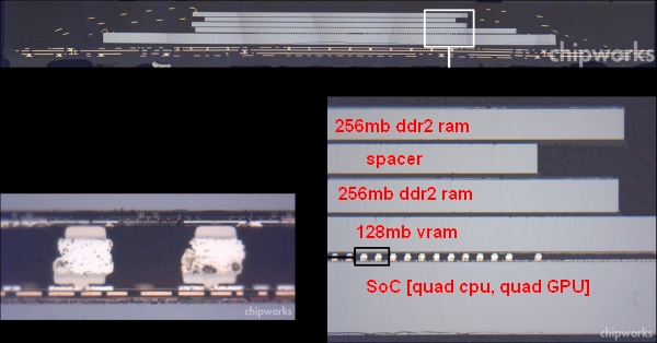
There are curious elements of the research, like the use of old process node designations and some stock media/old chip images that don't point to this being a huge production on the part of AMD.

There were a few benefits, aside from the higher bandwidth in the stack. There was slide that mentioned taking advantage of limited interposer area (slide 8).
A HMC-derived system is going to have logic there anyway, and exascale demands power efficiency scaling beyond what AMD--or possibly anyone--has been doing recently.


The whole PIM paradigm the paper suggested is based on HSA and NUMA, which means now the memory of the node (if we consider all PIMs tightly coupled to the host chip a node) is fragmented into several big, non-interleaved chunk.
It assumes a HMC-type arrangement, which already abstracts memory behind a packetized bus where each cube is its own node.
At the likely capacities and bandwidths involved, it may not be a significant problem for some possible AMD products, like game devices.
The host links are given an assumed 160GB/s. If we assume a 4GB stack in the same time frame (maybe), then something like a 60 FPS game would be incapable of accessing the whole DRAM anyway. It would require a double-capacity stack to say the same for 30 FPS, which might be a stretch for a generation or two.

I'm not sure of the impact that the proposal only gives the on-stack bandwidth as 4x higher.


Then the middleware built on top of the HSA runtime will be responsible of ping-ponging things and managing data placement among the PIMs.
It probably could, but probably should avoid doing that frequently.
These are multi-GB slices, which is a lot to move around and a lot of leeway for blocking or tiling.
GPU architectures are already tiled, and their tile sizes and even massive chunks of working set would find a decent fit. ROP-like functionality and various forms of atomic ops would be right at home.

The paper seemingly does not address the cache coherency issues, by the way. But as the whole thing is in a NUMA paradigm and the accesses to the memory is always destined to a single stack, perhaps a directory in the PIM would be needed... eh?
The likely way around this is the use of HSA, which has a more relaxed memory model.
It doesn't seem like the PIMs can access each other's nodes, so the stack logic has a different and local view of the stack's GBs of memory, making their share a form of mapped device memory.
Only the host would be able to see a much larger address space.

The host would need to be aware of how to interact with the memory allocated in this fashion.
There's already differing mapping behavior and interleaving settings handled by the memory controller and APU logic already for Garlic and standard memory, although this would be another layer of complication.

P.S. The inter-PIM interconnect wasn't mentioned in the written paper, it seems. Or did I miss something?
Slide 11 has it in its diagram. It's a very tiny mention, but consistent with an HMC-like design.

Is there more tho this than reducing power by moving the compute/memory closer? The logic dies in PIM stack seem suspiciously like garden varierty SoCs.
Bandwidth can be higher as well, direct stacking can have higher connection density, greater speeds, and lower signalling distance relative to an interposer.
The other is finding a way to get more out of limited interposer area.
It basically favors certain operation types that need a lot of memory movement, but can skimp on logic activity. Other workloads that don't have this requirement can have the host die that is unencumbered by the thermal and power limitations of the stack.
 
hmmm PS Vita has a curious multilayer chip on interposer, there are some nice pics around about that.
Still, I think the layers communicate on the border there, and not with a vertical bus.
Anyway, that should be possible to add, I suppose.

newpicture3p1i1l.jpg


SoC communicates directly to 128mb of Vram, but rest of the main pool is accessed via "bridges" from the sides.
 
Mods should rename the Volcanic Islands thread to Sea Islands and this thread to Volcanic Islands.
 
Back
Top