at least now there's party chat?
You need the day one update for that. But you can use your PS4 whilst that is downloading etc. Also you can download it now and install it from a USB stick.
at least now there's party chat?
")
I'm not sure what the figure is, I was thinking 2W per sandwich pair, each chip would be about 1W.You sure each GDDR actually burns 2W? Consider that the RAM on the rear side of Nvidia Titan boards don't have any cooling at all, and they run at a higher clock than PS4's.
We can only compare respective package sizes of the chips, of course. Die sizes will always be somewhat smaller.Our estimates of the XB1 APU were high (~410mm^2 vs the MS number of 363mm^2), since we are using the same techniques maybe we are overshooting again?

Do we know the final CPU and GPU clock speeds? And if not, is this something we will ever discover?
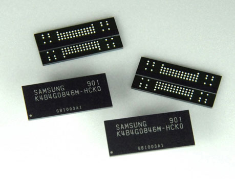
I tried to read the markings until my eyes bled, it's just a blob of pixelsHas anyone been able to ID the Samsung Memory Chip next to the Secondary Chip?
I'm guessing it's a 512MB chip?
I.e. based on package size it's (very roughly) ~400mm² vs. ~360mm²; but the chips obviously use different packaging ... so that result might be slightly deluding in the one or other direction.
Nice, but if that ~400mm² ended up being 363mm², then what might the ~360mm² be in reality?
I tried to read the markings until my eyes bled, it's just a blob of pixels
From the picture it's 7.5mm x 13mm so it matches ANY 16 bit DDR3 chip.
The smallest possible is 128MB, and the largest would be 1GB.
But even if it's 256MB, that makes a very good I/O buffer.
128MB : K4B1G1646G
256MB : K4B2G1646E or K4B2G1646C
512MB : K4B4G1646B
1GB : K4B8G1646B
I think it ends with E, so that would be the 256MB K4B2G1646E, but it's so fuzzy it's like a Rorschach Test.

Simply put that is what Sony does best. Then there are issue with DDR3 the traces on the mobo for every single memory chip needs to be the same length, that constrain doesn't exist with GDDR5.So how exactly is it that the PS4 can, as a whole, be significantly smaller than the competitor (with an internal power brick vs external) and still command a technical advantage?
I'm asking this as a complete novice, I honestly do not understand how there can exist any kind of size disparity between the two.
Pitcairn which include 20 CUs and 32 ROP and a 256 bit bus memory interface is 212mm^2 according to AMD. Looking at kabini die shot one can see that a jaguar cluster is not big at all.Should the PS4 APU not be bigger?
So how exactly is it that the PS4 can, as a whole, be significantly smaller than the competitor (with an internal power brick vs external) and still command a technical advantage?
I'm asking this as a complete novice, I honestly do not understand how there can exist any kind of size disparity between the two.
Should the PS4 APU not be bigger?