Xbox One (Durango) Technical hardware investigation

Status
Not open for further replies.
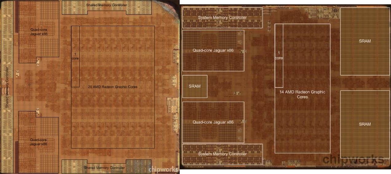
Looking at the Jaguar cores in each they look almost identical except for the extra bits in the corner of each Durango block. The same area for Orbis is blank.

What could that be? Would each CPU block have it's own audio core? Or would that be something else?

I'm not entirely convinced that it's not a matter of inconsistent box drawing.
The Orbis pic took the trouble to draw the line around the clock generator, while the Durango one drew through it.

Microsoft did state that it expanded the chip's on-die coherent interconnect, and those little blocks might be part of the customized interface.
 
If the regions in the pics were drawn with the same amount of care, those lighter areas would probably be outside of the x86 portion and part of the uncore.

The northbridge and interface sections seem to have had more freedom to vary, which makes sense to me. Both appear to have shied away from messing with the actual x86 sections.
 
That shocking moment when you realize that about 1/4th of the area marked as "quad core Jaguar" is what you used to think of as a CPU
 
There's a fair amount of logic attached to this SRAM pool, with its very own clock generator:

nZJF32p.png

The Audio Chip? it's connected to 64KB of SRAM.

Xbox_One_SoC_Audio_Wide.png
 
Looking at the picture - the block on the left doesn't look quite the same as the larger blocks on the right.

Is it possible that the GPU eSRAM is 'fast/big', whilst this is a denser/slower block for use in system functions? (maybe some DME functionality or kinect/HDMI/video encoder etc?)
 
Why is the XB1 xrays so dark compared to the other xb1 silicon xrays that are light ... And when you compare to the PS4 it doesn't look like a calibration issue ...

??

And I want a side shot !
 
in the same scale, the radeon core is a few bigger in xbox SoC.
A CU of Durango is slightly taller, but thinner. The layout is just different, for instance the SRAM banks for the registers and LDS got rotated by 90°. Guess this was an optimization to use the space as efficiently as possible.
Why is the XB1 xrays so dark compared to the other xb1 silicon xrays that are light ... And when you compare to the PS4 it doesn't look like a calibration issue ...
These pics are not x-ray images at all. ;)
And I want a side shot !
Will look the same as for the PS4 (it's a cut through the different metal layers):
Feature-top-Pic-682-021.jpg
 
Last edited by a moderator:
On same scale as Orbis:

ps4_xb1_die-vergleich1dadx.png

Are there two SRAM blocks or three? (One in the CPU and is it one or two in the GPU block? Is the SRAM in the GPU two identical blocks with one or two identical controllers? There are two identical looking blocks between the two big SRAM pools. Could explain cases of double the bandwidth, theoretically, if there are two blocks and one memory controller per block/two controllers total.)

If it is ~100 GB/Sec for each that is pretty interesting. I don't think the ~100 or the 192 or the typical 140/150 case numbers were talking about this new additional SRAM block at all, right? So peak theoretical eSRAM bandwidth could actually be around 300 GB/Sec?

Where did the 2560KB come from? And does anyone know how dense is AMD Jaguar L2 cache relative to SRAM?


Now what does that additional SRAM block do?


Any sign of the other eDRAM techniques (additional logic) in there?
 
I'm not sure if this is relevant or just coincidence, but it is interesting to note that unlike all previous AMD chips with integrated memory controllers (as well as the pre-ring bus Intel Nehalem and Westmemre 6C) the northbridge/UNB/crossbar is not adjacent to the memory controllers in the Xbox One SoC die.

Perhaps this has something to do with the extra SRAM next to the northbridge area.

Is this something along the lines of one being (pre)HUMA generation N and the other generation N+1?

Or is it HUMA (flavor X) versus MS idea of HUMA?

Is the extra SRAM a managed L3 cache or local memory (on the CPU side like the eSRAM on the GPU side?)
 
Last edited by a moderator:
Pick your theory, Both ended up with similar designs because of both companies had similar goals (One soc, good enough performance, ease of game development) or industrial espionage

With Buran URSS argued the former :LOL:


091-Atterrissage-Landing-bbur7.jpg
 
Could sRAM be L3 , like what is in Kaveri and Power8?

In relation to the sRAM sitting between the 2 jaguar modules ...


At the past Hotchips we saw IBM's Power8 use an L3 cache that sits between the cores..

ibms_power8.jpg


Near the other extreme is IBM’s POWER8 microprocessor (Figure 2), described by IBM Chief Nest Architect Jeff Stuecheli. The 650 mm2, 22 nm chip comprises 12 POWER-architecture CPU cores, each with 32 KB of instruction and 64 KB of data cache. Each core also has its own 512 KB of SRAM L2 cache, and the 12 L2s share an enormous 96 MB of embedded-DRAM L3. Stuecheli said the three levels of coherent cache could sustain 230 gigabytes per second (GBps) of aggregate memory bandwidth. Interestingly, the chip also contains a small transactional memory. - See more at: http://www.altera.com/technology/sy...ot-chips-conference.html#sthash.9OW7Yyl4.dpuf

Also in Kaveri we see L3 sRAM cache making an appearance ...
 
Status
Not open for further replies.
Back
Top