One thing I've been mulling over concerning perf/mm2 is that top-end comparisons usually work because we compare designs on mostly comparable processes, or their direct predecessors.
With the rising costs and lengthening delays in making node transitions, and the lack of guarantees that making a transition is beneficial, perf/mm2 analysis may become more complicated.
AMD made a conscious decision prior to the 32nm cancellation that its lower-end chips would remain on 40nm, because of the cost argument.
28nm has not yet given us the volumes or perf/$ many have expected.
AMD may be pressured to lower prices or roll out some kind of OC edition, but supply limitations may push out the crossover point where any downward trend in demand crosses its supply.
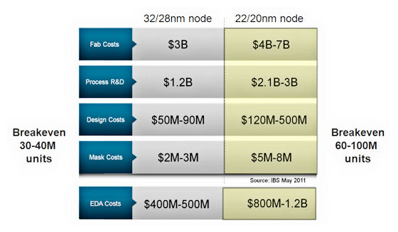
Slides were shown with chip design costs more than doubling from 45nm to 22nm, I'm not certain if that includes escalating mask costs.If 2.5 and 3D integration come to pass in wide scale, we may be comparing designs whose perf/mm2 per layer is inferior, but whose cost/mm2 and cost per design is competitive.
While it is generally not considered elegant or efficient to throw a lot more silicon at something, it doesn't look so bad if--and I am not claiming this is true yet--you can achieve the same end result while pocketing some cash savings.
When silicon scaling does hit a wall, we may have to start comparing perf/mm3 or perf/elements used in the recipe as designers and fabs work their way around any impediments.

 )
)