Haswell vs Kaveri

Perhaps this is a cut back version of Kaveri with only 512 shaders. I'll make the wild guess that they originally planned something with 768 shaders on a different socket or BGA with GDDR5, but cut down on execution risk by using their existing socket. The limited memory bandwidth would have meant that 768 shaders wouldn't have been properly fed so they went with 512 instead.


I don't think so. 512 SPs was confirmed long time ago.


Only ~100gflops for the CPU? No AVX2/FMA? I guess it's only 2 "modules" of FP compute, but that's still well lower than a dual core Haswell.

Numbers from a different forum:

CPU - 3,7GHz x 4 Cores x 8 = 118,4 GFLOPs
GPU - 0,72GHz x 512 Cores x 2 = 737,3 GFLOPs


Gflops isn't all, GCN should do much better than Intel Gen7.5 at the same Gflops especially when using MSAA. Of course, Gen8 should change this with the big redesign. 850 Gflops for the whole APU is less than AMD predicted a long time ago.
 
I'm really looking forward to see CPU/GPU interop on Kaveri. This was a main weakness in past APUs compared to Intel.
 
CPU - 3,7GHz x 4 Cores x 8 = 118,4 GFLOPs

Wouldn't it be more like:

CPU - 3,7GHz x 2 FPU x 16 = 118,4 GFLOPs

The CPU looks to be more than a match for the Jaguars in the consoles but the CPU is barely over half of the XB1 GPU with a far inferior memory setup.

This thing might run next gen 720p/60fps console ports at 480p/30fps though. So not bad for the lowest level of entry to PC gaming.
 
why do people find this so hard....lol

there are 2 128bit FMA units per module. 2 modules on the SOC

so 4*2*2*2*3.7ghz

2 Modules each with 1 FPU each with 2 128 bit FMAs so that's 4 single precision floating point numbers per cycle at peak per FMA.

Looks like it ought to be 4 SP Words * 2 FMAs * 2 Modules * 3.7 ghz ~ 59 GFLOPs to me unless they increased the width of the FMAs or doubled up on the FPUs per module.
 
Last edited by a moderator:
FMA = 2 flops/cycle.
128-bit FMA = 8 flops/cycle.
2 128-bit FMAs = 16 flops/cycle.
2 Modules = 32 flops/cycle.
Total flops = 32 * 3.7 GHz = 118.4 Gflops
 
Gflops isn't all, GCN should do much better than Intel Gen7.5 at the same Gflops especially when using MSAA. Of course, Gen8 should change this with the big redesign. 850 Gflops for the whole APU is less than AMD predicted a long time ago.
Sure, totally agreed. Just given that I don't have one to play with all I have for now are theoretical numbers :) The GPU side sounds like it's in the right ballpark for performance, I'm mainly surprised by the CPU part (but admittedly am kind of a BD/PD noob). There the raw Gflops difference is much more significant IMO.

Thanks for the slide links. I'm not sure I get the point of some of them without notes/surrounding audio, but good overall idea. They aimed a little low with the GT630 comparison, but maybe they were just trying to make it very obviously better to people on-site. Eagerly awaiting reviews.
 
Last edited by a moderator:
Sure, totally agreed. Just given that I don't have one to play with all I have for now are theoretical numbers :) The GPU side sounds like it's in the right ballpark for performance, I'm mainly surprised by the CPU part (but admittedly am kind of a BD/PD noob). There the raw Gflops difference is much more significant IMO.

With Bulldozer, AMD brought forth an FPU architecture that heavily banked on FMA to give it satisfactory performance, whereas Intel went with wider SIMD. Only the 8 core was within the same realm as Sandy Bridge. Since AMD has not advanced its FPU at all since and the server and 8-core desktop level has flatlined for the disclosed future, we can assume everything new is half as inspiring as Bulldozer in terms of FP performance.

One of the areas where Bulldozer wasn't beaten by SB was an unexpected level of performance in integer SIMD, which was in part enabled by the delayed promotion of integer ops until AVX2.
I'm keeping an eye on this because AMD has indicated that it "streamlined" the FPU, which might have cut down that area of unintended competitiveness.
Some of the other preliminary details indicated there might have been other regressions, but those were hard to verify.
Since AMD has shown zero movement in the eight core arena, we can cut everything in half since the APUs stop at four.
 
I'm keeping an eye on this because AMD has indicated that it "streamlined" the FPU, which might have cut down that area of unintended competitiveness.
According to GCC src files SR (bdver3) got 3 ports instead of 4 but with an added shuffling unit.
bdver73ul1.png
 
The peak integer throughput case goes down, as well as how much MMX and FP can go on concurrently.
Removing that port might have reduced the number of operands needed from the register file, although the clock speed regression doesn't indicate the savings went into timing improvement.
The additional port in BD gave more MMX capability that wasn't under frequent contention.
The use cases that showed BD's relative strength in MMX may see a regression.

There would be improvements in other code, if the shuffle unit takes some burden off that heavily used XBAR unit.

Using FP and MMX in the same module is going to hurt more this time around.
 
Last edited by a moderator:
(my wild guess)

the less ports you have, the higher should be the utilization of the remaining ones, kinda like VLIW4 vs VLIW3.
and
more ports can also lead to less balanced load on the load/store units, issuing ffma+ffma+fmal+fmal is a lot of data and it's not likely all instructions to work on registers for a long time.

so there is instruction and data parallelism working against more ports.
 
the less ports you have, the higher should be the utilization of the remaining ones, kinda like VLIW4 vs VLIW3.
That's an argument used when trying to say that a regression isn't that bad, or if it is bad that it's limited enough to awkwardly handwave away.
The higher MMX throughput cases are themselves a limited set, just ones where BD wasn't that bad.
In terms of their throughput, whether all the ports are generally used is a Do Not Care.

If the savings somehow allowed for more units (no) or higher clocks (no), it might mean more.
It might mean less area, which might mean cheaper for AMD.

more ports can also lead to less balanced load on the load/store units, issuing ffma+ffma+fmal+fmal is a lot of data and it's not likely all instructions to work on registers for a long time.
The FPU does not have direct access to the L/S units, just a buffer.
The L/S units would see no difference, other than the possibility they see less activity because of the reduced throughput.
 
They should have just compared Kaveri to Intel's Iris Pro 5200, not a GT440 (GT630).
But then again Kaveri's real competition will be Broadwell.
 
The peak integer throughput case goes down, as well as how much MMX and FP can go on concurrently.

Are you saying that integer throughput will be affected by lower floating point throughput in mixed code because of more contention for resources upstream in the pipeline in mixed code sequences?
 
They should have just compared Kaveri to Intel's Iris Pro 5200, not a GT440 (GT630).
But then again Kaveri's real competition will be Broadwell.
Well if it's coming January I think a comparison to the R-series Iris Pro parts is definitely reasonable. That's likely the most direct competition architecturally although I expect AMD to be pretty competitive on pricing as they need to grab market share with Kaveri.
 
R-series isn't a mass product whereas Kaveri is. Not really comparable. At least in the desktop space. Intel has to bring something decent for the socket version which happens with Skylake at the earliest if they want compete. Mobile as always is completely different of course.
 
I meant integer SIMD.

Gotcha. SIMD/FPU takes a small step back this gen but that's understandable since steamroller is designed to go into a consumer APU. They won't even have a 4 module steamroller part for supercomputing and simulation. Looking forward to seeing what kind of gains we get from the improvements they made to how the main integer pipeline's program flow is handled.

I'm also wondering how quick and easy it would be to use the GPU for floating point work, whether a compiler could be written which would know how to automatically utilize the GPU for certain types of floating point work or whether they'll have a math kernel library for GPU work now. I haven't heard of any new instructions for Kaveri yet which must be necessary for issuing commands to the GPU and memory handling by the GPU.

I guess what I'm asking what exactly makes Kaveri easier to program than Trinity from the perspective of a higher level language? Is it just faster, are debugging tools better?
 
Last edited by a moderator:
Gotcha. SIMD/FPU takes a small step back this gen but that's understandable since steamroller is designed to go into a consumer APU.
I think some of the best case for integer SIMD is software media codecs, which is still in the consumer fold. The hardware/GPU media paths tend to have tradeoffs in quality.

I'm also wondering how quick and easy it would be to use the GPU for floating point work, whether a compiler could be written which would know how to automatically utilize the GPU for certain types of floating point work or whether they'll have a math kernel library for GPU work now. I haven't heard of any new instructions for Kaveri yet which must be necessary for issuing commands to the GPU and memory handling by the GPU.
In theory, HSA and specialized APIs can help with this, however it is not transparent and it's not clear how much can be done on the fly.

I'm not feeling confident that Steamroller or GCN are where they need to be for the GPU to make up for the FPU.
Barring some unforseen dynamic routing, Kaveri is going to look like a weaker Richland.
Barring some advance in the wide gulf in latency, SIMD granularity, and cache behavior of the CPU and GPU, there's going to be a swath of workloads that do not do well on the GPU.
For heterogenous loads, there will be those with latency requirements or mediocre speedups that cannot tolerate the overhead of hopping between the sides.
Then there's all the software that was and will not be coded specially for a minority holder of the x86 market.

Those just get the non-improvement of Kaveri.
I suppose we'll have to see how much will fall in each bucket.

I guess what I'm asking what exactly makes Kaveri easier to program than Trinity from the perspective of a higher level language? Is it just faster, are debugging tools better?
There is hardware support for queueing and memory sharing.
The GPU architecture is potentially no longer in the "downright unacceptable" category.
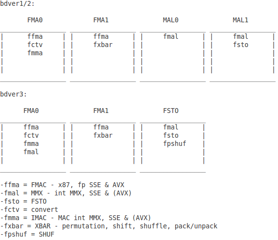
 
Back
Top