
That's probably happening in the Denver version, now they know it works on T124.
Wow!

That's probably happening in the Denver version, now they know it works on T124.
I cant tell if you are taking the piss or not .... seriously... wow
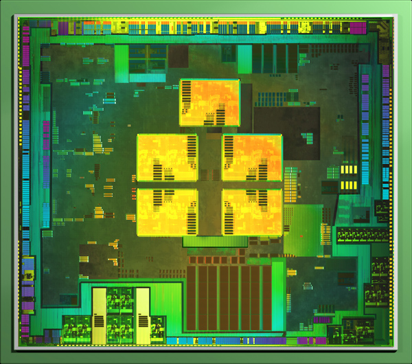
I order that the joke doesn't spread any further as truth, I'll come clean: The image and subsequent analysis are completely fabricated. I recently finished the analysis of the real die shot and wanted to make a joke, because I now understand first-hand how bad the marketing image is, and how nonsensical some of the analysis of Tegra K1 is. Financial analysts with monetary stakes in NV and/or competitors getting the areas completely wrong, etc.
There is one piece of information in the shot that's correct if you know what you're looking at, but otherwise it's as made up as the original, as is the analysis in the same post, and the rest of my contribution to the thread after it.
You can mix transistor variants on the same wafer (LP + HPM for example), but you can't mix major nodes.
I think the joke was too convincing for some (and yeah, we edited Alexko's post to have less laughs to keep the joke going)
Are those CPU cores actually to scale on their public "die shot," if you can even call it that? Nvidia obfuscates and doctors their Tegra die shots so heavily, that I can't help but feel like you've wasted your time.I'm still working on it and should have more information to share in a few months.
 ), coincidentally the same number as Tegra K1. Tegra K1's "die shot" has copy-pasted "artist's representations" of GPU cores.
Aw man. Well, at least others can see why it was a farce.I order that the joke doesn't spread any further as truth, I'll come clean: The image and subsequent analysis are completely fabricated. I recently finished the analysis of the real die shot and wanted to make a joke, because I now understand first-hand how bad the marketing image is, and how nonsensical some of the analysis of Tegra K1 is. Financial analysts with monetary stakes in NV and/or competitors getting the areas completely wrong, etc.
There is one piece of information in the shot that's correct if you know what you're looking at, but otherwise it's as made up as the original, as is the analysis in the same post, and the rest of my contribution to the thread after it.
You can mix transistor variants on the same wafer (LP + HPM for example), but you can't mix major nodes.
I think the joke was too convincing for some (and yeah, we edited Alexko's post to have less laughs to keep the joke going)
I'm sure he'll come back saying he was playing alongThe joke spread to Intel/Nvidia fanboy-land: http://forums.anandtech.com/showpost.php?p=36454451&postcount=146
Obviously they took the story very seriously
I'm sure he'll come back saying he was playing along
Anyway, I think he was just trying to see if he could fool a few people. There's some guys over there pumping Tegra K1 like it's the second coming of G80 or something.
The real die is completely different to the marketing shot. The A15s are big (even the companion core), the SMX is visually distinct from the rest of the GPU, etc. I mean, even on the marketing picture you should instinctively know that there's more to a GPU than just ALUs. In this config of Kepler it might even be instinct that they might not dominate the area.
They usually don't publicly publish them at all. They have plenty of SoC analysis and die shots which are only available for purchase only.Chipworks are usually the ones to publish the die shots, but AFAIK they haven't done that for Tegra K1, yet.
The real die is completely different to the marketing shot. The A15s are big (even the companion core), the SMX is visually distinct from the rest of the GPU, etc. I mean, even on the marketing picture you should instinctively know that there's more to a GPU than just ALUs. In this config of Kepler it might even be instinct that they might not dominate the area.
) in my idiotic layman's defense I did actually ask WTF TMUs, ROPs or FP64SPs are....I'm sure he'll come back saying he was playing along