
109GB/s above is the minimal bandwidth but he talked about how the maximal theoretical bandwidth can't be rarely achieved. As he compares that to Sony's I assume he probably means 140-150GB/s number MS mentioned for some rare but "real" r/w cases. So your 93GB calculation is based on wrong data.
You are using an out of date browser. It may not display this or other websites correctly.
You should upgrade or use an alternative browser.
You should upgrade or use an alternative browser.
The pros and cons of eDRAM/ESRAM in next-gen
- Thread starter Shifty Geezer
- Start date
109GB/s above is the minimal bandwidth but he talked about how the maximal theoretical bandwidth can't be rarely achieved. As he compares that to Sony's I assume he probably means 140-150GB/s number MS mentioned for some rare but "real" r/w cases. So your 93GB calculation is based on wrong data.
No. 109GB/s is a peak number without any simultaneous read and write, like the 176GB/s peak number, not a minimum or average number. Devs usually get 70% to 80% of real average number with most given peak BW numbers. Interestingly 120/140GB/s is roughly 70%/80% from 176GB/s and I took a best case, without memory contention, with 80% from the 109GB/s.
What I did not take into account is the main DDR3 ram. But it gets tricky and is even more apples and oranges because it's now fully impacted by memory contention (and a great deal apparently judging by the Microsoft's slide) and some BW is lost during the memory tiling needed in such complex memory architecture, but here we don't have any real data unfortunately.
From what I understand about bandwidth and memory architecture, and here it would be really interesting to have feedback from developers, please feel free to contradict me: my logical assumption is that: the more the games are fullHD and/or complex and/or open world, the more you need to use memory tiling on XB1, the more you lose total average BW on both DDR3 and esram memory bus.
This conversation has taken a sudden turn off course.
Sony's numbers are unlikely to be an average, as that would be pointless in context of the slide. Sony are trying to demonstrate - specifically - how much BW the GPU can realistically use given certain levels of BW consumption from the CPU.
It's demonstrating the contention issue, not trying to give out a pointless bit of information to be used in forum wars.
"Rare" in the case of the Xbox is explained as "usually with simultaneous read and write, like FP16-blending".
That's not an approximation or an estimate, it's you making a figure up.
The point is that operations or combinations of operations that require more BW (read modify write and simulatneous read and write) are the ones that can get more transfers from the system.
Arguing over BW figures for the sake of having the highest number is counter-productive. Under BW bound GPU operations the Xbox One can move as fast or faster than a similar GDDR5 equipped system, but this is only one particular set of circumstances.
The Sony figure was not intended to be used in the manner in which you're using it, and the Xbox figure is simply one you've made up.
BW has to be there when you need it or it's irrelevant.
These figures are entirely consistent with the figures and examples that MS has publicly released.
The key word is rarely. Sony's 120/140GB/s number are genuine average number when those 140-150GB/s esram number are achieved rarely. What is the definition or "rare"?
Sony's numbers are unlikely to be an average, as that would be pointless in context of the slide. Sony are trying to demonstrate - specifically - how much BW the GPU can realistically use given certain levels of BW consumption from the CPU.
It's demonstrating the contention issue, not trying to give out a pointless bit of information to be used in forum wars.
"Rare" in the case of the Xbox is explained as "usually with simultaneous read and write, like FP16-blending".
We could do a rough approximation though. If "rarely" means 10% of the time then we could average a number we could compare with Sony's numbers (120-140GB/s):
- 70%-80% of 109GB/s = 76/87GB/s 90% of the time but we'll take the higher number because no contention with CPU so 87GB/s.
- 145GB/s (highest esram BW under rare conditions) 10% of the time (rarely)
That's not an approximation or an estimate, it's you making a figure up.
The point is that operations or combinations of operations that require more BW (read modify write and simulatneous read and write) are the ones that can get more transfers from the system.
Arguing over BW figures for the sake of having the highest number is counter-productive. Under BW bound GPU operations the Xbox One can move as fast or faster than a similar GDDR5 equipped system, but this is only one particular set of circumstances.
Average estimated esram really usable BW = 93GB/s that you can now compare with 120/140GB/s. Of course you have to add main ram BW (which has contention here) but then we'll have to add also the esram + ddr3 BW lost by the data transfers during memory tiling etc.
The Sony figure was not intended to be used in the manner in which you're using it, and the Xbox figure is simply one you've made up.
Of course it is supposing "rarely" means at least 10% but it may even means less than 10%, and I really doubt rare means more than 1/10.
BW has to be there when you need it or it's irrelevant.
But it's the first time a developer admits in an interview that those BW microsoft numbers, even if true, are a bit dishonest (because it's apples and oranges stuff) and can only be used rarely, under rare conditions.
These figures are entirely consistent with the figures and examples that MS has publicly released.
No. 109GB/s is a peak number without any simultaneous read and write, like the 176GB/s peak number, not a minimum or average number. Devs usually get 70% to 80% of real average number with most given peak BW numbers. Interestingly 120/140GB/s is roughly 70%/80% from 176GB/s and I took a best case, without memory contention, with 80% from the 109GB/s.
Under what conditions do you see the Xbox One being BW bound by the esram for reads, writes or reads and writes?
BTW, any access that was soley reads or writes should have a highly favourable access pattern and be able to get very close to the maximum possible usage.
What I did not take into account is the main DDR3 ram. But it gets tricky and is even more apples and oranges because it's now fully impacted by memory contention (and a great deal apparently judging by the Microsoft's slide) and some BW is lost during the memory tiling needed in such complex memory architecture, but here we don't have any real data unfortunately.
Both the Xbox One and PS4 are affected heavily by CPU and GPU contention on main memory accesses. The esram is unaffected by this.
Xbox one doesn't necessarily use any additional BW is copying to or from esram - it depends entirely on how the game uses the esram. Tiling doesn't necessarily use any more esram<->ddr3 BW than not tiling either.
Tiling in a deferred renderer is not necessarily the same thing as tiling to fit a large buffer into two or more slices on the 360.
The unfortunate thing is that Xbox One doesn't have 48 or 64 MB of embedded ram, so it can store texture data for the upcoming frames in there (for example in a virtual texturing texture atlas).
With all buffers (except perhaps shadow) and almost all texture reads coming from esram, esram BW utilisation would consistently be higher and main memory contention issues could be further reduced.
With all buffers (except perhaps shadow) and almost all texture reads coming from esram, esram BW utilisation would consistently be higher and main memory contention issues could be further reduced.
No. 109GB/s is a peak number without any simultaneous read and write, like the 176GB/s peak number, not a minimum or average number. Devs usually get 70% to 80% of real average number with most given peak BW numbers. Interestingly 120/140GB/s is roughly 70%/80% from 176GB/s and I took a best case, without memory contention, with 80% from the 109GB/s.
What I did not take into account is the main DDR3 ram. But it gets tricky and is even more apples and oranges because it's now fully impacted by memory contention (and a great deal apparently judging by the Microsoft's slide) and some BW is lost during the memory tiling needed in such complex memory architecture, but here we don't have any real data unfortunately.
From what I understand about bandwidth and memory architecture, and here it would be really interesting to have feedback from developers, please feel free to contradict me: my logical assumption is that: the more the games are fullHD and/or complex and/or open world, the more you need to use memory tiling on XB1, the more you lose total average BW on both DDR3 and esram memory bus.
Read the XB1 architect interview:
With DDR3 you pretty much take the number of bits on the interface, multiply by the speed and that's how you get 68GB/s. That equivalent on ESRAM would be 218GB/s. However, just like main memory, it's rare to be able to achieve that over long periods of time so typically an external memory interface you run at 70-80 per cent efficiency.
http://www.eurogamer.net/articles/digitalfoundry-the-complete-xbox-one-interview
hm? Shadow buffers would be good to have in the scratchpad.
But how you gonna fit them bro?
I've been getting all inspired by sebbbi, and his talk of intelligently re-using sections of large shadows. Made me think that main ram might be the place to stick 'em. Low write BW, and only sampling what you need for the frame.
Wait a minute ... could you bake sections of a huge, dynamically generated (and intelligently re-used) shadow into your texture atlas thingy...?
Read the XB1 architect interview:
http://www.eurogamer.net/articles/digitalfoundry-the-complete-xbox-one-interview
Yes you are right, my bad, it's written 70/80% of 219GB/s, hence 153/175GB/S on genuine average BW for esram apparently.
How could I have missed this interview?
shredenvain
Regular
What's the point of the high bandwidth if the low clocked and CU/ROP limited GPU can't effectively use it?
Low clocked compared to Desktop cards?
Also from what I have read from sebbbi the extra bandwidth would be beneficial when using
Compute shaders that utilize Rops. Also the system doesnt have enough bandwidth to fully use 32 Rops. 32 rops would have given them overhead though.
liquidboy
Regular
Found a 2008 post from Microsoft-DirectX Miller on an interesting topic of "I just tried to use four render targets on my Xbox 360 (EDRAM) and it failed!!" ...
I know its xb360 and over 6yrs old, but I wonder if the logic still stands and can be extrapolated to XB1's ESRAM...
MS architects did go on record and say that XB1 design is effectively fixing issues they encountered with EDRAM in XB360 an evolution on XB360s design + learnings......
Anyway I found it interesting")
Article
I know its xb360 and over 6yrs old, but I wonder if the logic still stands and can be extrapolated to XB1's ESRAM...
MS architects did go on record and say that XB1 design is effectively fixing issues they encountered with EDRAM in XB360 an evolution on XB360s design + learnings......
Anyway I found it interesting
Article
Yes you are right, my bad, it's written 70/80% of 219GB/s, hence 153/175GB/S on genuine average BW for esram apparently.
How could I have missed this interview?
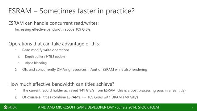
As of June 2nd 2014 the highest bandwidth achieved by a developer so far was for a single read/write heavy post processing pass at 141GB/s. While a developer may reach a record of 153GB/s for some operation at some point in the future, it won't be the average developers achieve.
PS4 & Xbox One have different strengths and weaknesses in different manners regarding their memory systems.
Last edited by a moderator:
The esram is very different to a typical dram bus in that effective bandwidth drops on a typical dram bus as competition between reads and writes increases, but on Xbox One effective bandwidth increases. This is important as a mixture of reads and writes is *exactly* the type of situation that places the highest demand for bandwidth on memory.
109 GB/s is already high for exclusive use of a GPU of Xbox one's power. That is can increase significantly under the most demanding use cases is actually pretty cool and desirable and not something to be sniffed at.
And 141 GB/s is for a specific case - a post process filter. Add in some reads and writes from the multiple DMA units and it could probably go higher. And for a synthetic case of FP16 blending and favourable DMA transfer patterns and it may go higher still.
The thorns in Xbox One's shoes are esram size and main memory BW and contention. The esram appears to be very well suited to it's intended task.
The thorns in Xbox One's shoes are esram size and main memory BW and contention.
Those are big thorns.
I'd expect that the somewhat small size of the esram means that in practice it gets treated like manually managed cache -- and most of the data that ends up there likely depends in part on data that must be taken first from main memory.
That doesn't mean it can't be made to work well. But if the experience of the PS3 is any guide, it will take programmers a good deal of effort to get the most out of it.
The esram is very different to a typical dram bus in that effective bandwidth drops on a typical dram bus as competition between reads and writes increases, but on Xbox One effective bandwidth increases. This is important as a mixture of reads and writes is *exactly* the type of situation that places the highest demand for bandwidth on memory.
109 GB/s is already high for exclusive use of a GPU of Xbox one's power. That is can increase significantly under the most demanding use cases is actually pretty cool and desirable and not something to be sniffed at.
And 141 GB/s is for a specific case - a post process filter. Add in some reads and writes from the multiple DMA units and it could probably go higher. And for a synthetic case of FP16 blending and favourable DMA transfer patterns and it may go higher still.
The thorns in Xbox One's shoes are esram size and main memory BW and contention. The esram appears to be very well suited to it's intended task.
109GB/s is only a peak number, similar to the 176GB/s PS4 peak number. But as there is not contention with CPU we can suppose a great average BW can be reached like ~80%.
141 GB/s is a "current record holder", number provided by Micrososft, everything accounted for as it should. And DMA units are not BW free (they are CPU free), if you transfer data DDR3 <-> esram, you will eat DDR3 and esram total BW.
109 is for either reads or writes. We don't know what percentage of this can be used practically, but its unlikely to matter much in practice as its unlikely to be a bottleneck. In practice GPUs are likely to need a combination of reads a writes, and in doing so have access to far more than 109 should they need it.
141 wasn't from an attempt to win a record, it's part of a production title. The point about DMA is that it could add additional reads and writes to ongoing GPU operations and so see effective earam BW utilisation rise. DMA is obviously not BW free.
Esram BW is a definite strong point for Xbone.
141 wasn't from an attempt to win a record, it's part of a production title. The point about DMA is that it could add additional reads and writes to ongoing GPU operations and so see effective earam BW utilisation rise. DMA is obviously not BW free.
Esram BW is a definite strong point for Xbone.
LightHeaven
Regular
What's the point of the high bandwidth if the low clocked and CU/ROP limited GPU can't effectively use it?
The point is because it can use it
In fact, it's possible for them to be bandwidth bound too.It is not true because you can't compare those numbers (apples and oranges): from the Metro Redux interview of Oles Shishkovstov:
The key word is rarely. Sony's 120/140GB/s number are genuine average number when those 140-150GB/s esram number are achieved rarely. What is the definition or "rare"?
They also have said that they worked with infant SDKs and with very little time. So yeah, for them, it might be rare to achieve peak usage of esram, but that does not mean it's the same for everyone, or that it won't improve with better apis to manage that. Unless there's something inherently from the design preventing the esram bandwidth to be sustained, it most likely will be in upcoming years.
oldschoolnerd
Newcomer
109 is for either reads or writes. We don't know what percentage of this can be used practically, but its unlikely to matter much in practice as its unlikely to be a bottleneck. In practice GPUs are likely to need a combination of reads a writes, and in doing so have access to far more than 109 should they need it.
141 wasn't from an attempt to win a record, it's part of a production title. The point about DMA is that it could add additional reads and writes to ongoing GPU operations and so see effective earam BW utilisation rise. DMA is obviously not BW free.
Esram BW is a definite strong point for Xbone.
I think the x1 design is based around the esram. There are contention issues when system ram has to service both a cpu and a gpu simultaneously. In order to extract the maximum performance the gpu needs to use the esram exclusively, relying on tiling and the asynchronous data move engines to ensure that all the data required by the gpu is moved to and from system ram in a timely manner. This is the fourth stage of esram utilisation that was on that MS slide recently. I think the hardware has been designed with this in mind.
The Metro dev said that the x1 suffered as the gpu and cpu could not access system ram concurrently, however this issue would be mitigated by the gpu using the esram exclusively. This is important because though the data move engines may still stall accessing the system ram, the gpu will not stall as its working set is in esram.
Clearly non-trivial to achieve in practice!
liquidboy
Regular
109GB/s is only a peak number, similar to the 176GB/s PS4 peak number. But as there is not contention with CPU we can suppose a great average BW can be reached like ~80%.
141 GB/s is a "current record holder", number provided by Micrososft, everything accounted for as it should. And DMA units are not BW free (they are CPU free), if you transfer data DDR3 <-> esram, you will eat DDR3 and esram total BW.
as the architects have stated numerous times
Nick Baker: Over that interface, each lane - to ESRAM is 256-bit making up a total of 1024 bits and that's in each direction. 1024 bits for write will give you a max of 109GB/s and then there's separate read paths again running at peak would give you 109GB/s. What is the equivalent bandwidth of the ESRAM if you were doing the same kind of accounting that you do for external memory... With DDR3 you pretty much take the number of bits on the interface, multiply by the speed and that's how you get 68GB/s. That equivalent on ESRAM would be 218GB/s. However, just like main memory, it's rare to be able to achieve that over long periods of time so typically an external memory interface you run at 70-80 per cent efficiency.
The same discussion with ESRAM as well - the 204GB/s number that was presented at Hot Chips is taking known limitations of the logic around the ESRAM into account. You can't sustain writes for absolutely every single cycle. The writes is known to insert a bubble [a dead cycle] occasionally... One out of every eight cycles is a bubble, so that's how you get the combined 204GB/s as the raw peak that we can really achieve over the ESRAM. And then if you say what can you achieve out of an application - we've measured about 140-150GB/s for ESRAM. That's real code running. That's not some diagnostic or some simulation case or something like that. That is real code that is running at that bandwidth. You can add that to the external memory and say that that probably achieves in similar conditions 50-55GB/s and add those two together you're getting in the order of 200GB/s across the main memory and internally.
One thing I should point out is that there are four 8MB lanes. But it's not a contiguous 8MB chunk of memory within each of those lanes. Each lane, that 8MB is broken down into eight modules. This should address whether you can really have read and write bandwidth in memory simultaneously. Yes you can there are actually a lot more individual blocks that comprise the whole ESRAM so you can talk to those in parallel and of course if you're hitting the same area over and over and over again, you don't get to spread out your bandwidth and so that's why one of the reasons why in real testing you get 140-150GB/s rather than the peak 204GB/s is that it's not just four chunks of 8MB memory. It's a lot more complicated than that and depending on how the pattern you get to use those simultaneously. That's what lets you do read and writes simultaneously. You do get to add the read and write bandwidth as well adding the read and write bandwidth on to the main memory. That's just one of the misconceptions we wanted to clean up.
Andrew Goossen: If you're only doing a read you're capped at 109GB/s, if you're only doing a write you're capped at 109GB/s. To get over that you need to have a mix of the reads and the writes but when you are going to look at the things that are typically in the ESRAM, such as your render targets and your depth buffers, intrinsically they have a lot of read-modified writes going on in the blends and the depth buffer updates. Those are the natural things to stick in the ESRAM and the natural things to take advantage of the concurrent read/writes.
Digital Foundry: So 140-150GB/s is a realistic target and you can integrate DDR3 bandwidth simultaneously?
Nick Baker: Yes. That's been measured.
Realistic
140-150GB/s for ESRAM (internal)
50-55GB/s for DDR (external)
Total =190-205 GB/s
Similar threads
- Replies
- 141
- Views
- 14K
- Replies
- 50
- Views
- 15K
- Replies
- 61
- Views
- 9K
- Replies
- 13
- Views
- 4K