Wii U hardware discussion and investigation *rename

Status
Not open for further replies.
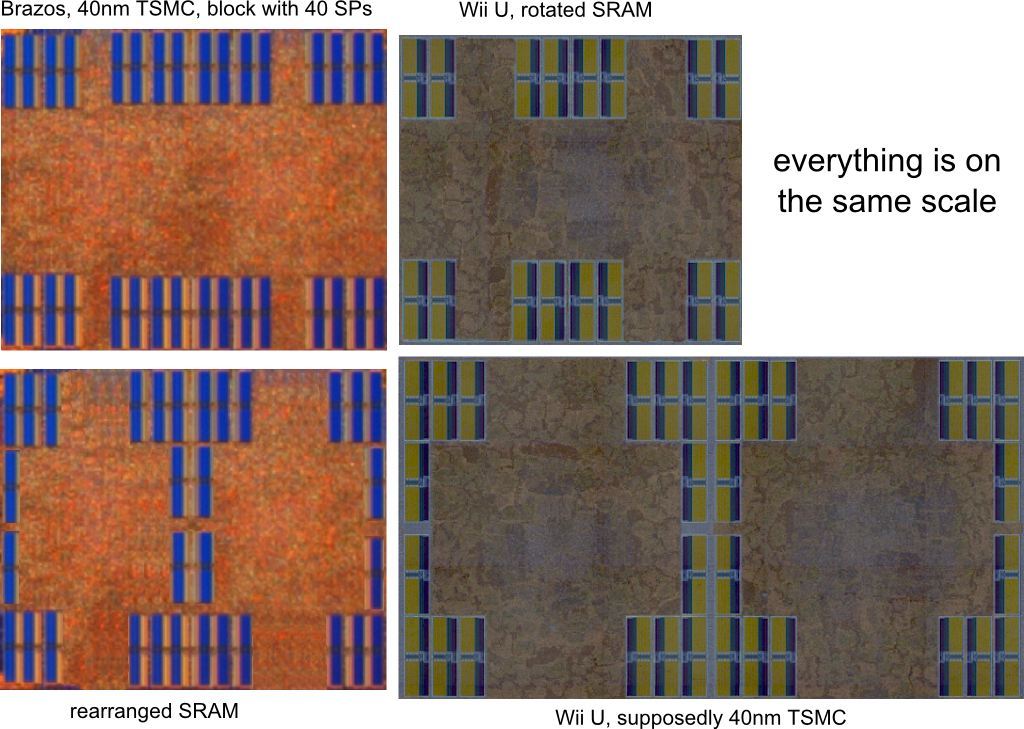
Our technical theories aren't all that technical. 160SPU's just seems like not enough to support what the Wii U has been pushing out. But then 320 would seem like an obvious advantage as well, but we would know it was 320SPU's if that was the case.

Really though, we're going off of barely there fumes.
 
Size

@ Esrever

On Page 191 (#4768) i tried to show that the surface with the logic (The areas without a visible structure of "Brazos" and "Latte") differs only ~12.4%. (Brazos > Latte)

So if "Latte" is on 40nm than it is more realistic to go with something like 320sp.

Or the whole scaling of the illustration of "Gipsel" is not correct.
 
I feel like I have to continually remind everyone that "40nm" is not universal, it's just a broad denotation trying to capture a large variety of parameters. One fab's so-called 40nm can be a lot denser than another's, and TSMC's is very dense. They even say their SRAM cells can go down to 0.2um^2, while NEC/Renesas (a strong candidate for Latte's fab) only claims 0.3um^2.

I'm sure this has been brought up before, but since we're mentioning 256 shaders has anyone done much of a comparison against Cayman? Here's a Trinity die shot:

http://images.dailytech.com/nimage/Trinity_Die_Shot.jpg

Shader blocks still look like the same rough layout. I can't find anything for HD 6950 or 6970, maybe someone else can.

I know we've all been steered to expect something much older but this should at least be technically feasible for the time frame in which Wii U was announced and released.

The idea that this GPU is very different from something AMD/ATI already designed is a very bizarre one, I can't see why that would be the case.. but I wouldn't put it past Nintendo.
 
So anyone want to list why they think its 320 shaders based on anything technical(the die shot or documentations)? Seems like people will believe what they want. The area is way too small to fit 320 at 40nm.
And too large for just 160. Either they increased the density of the layout a bit (entirely possible given the experience with TSMC's 40nm process, the low clock target, and the possibility of a lesser feature set compared to Brazos' DX11; the area is closer to the one expected for 320SPs than 160SPs), they changed the architecture, or it isn't 40nm TSMC. Or some combination.
The layout looks like 20 shaders per block with matching cache blocks. So whats the 40 shader block theory's basis at this point beside it being 50% larger?
wPPQWH2.jpg

This is with 2 Wii U blocks compare to 1 bobcat block. the size is larger sure but the notable features are the same...
I compared the possibilities already some time ago. They could have rotated the SRAM blocks and changed the pipeline a bit to get away with half of the blocks (larger SRAM banks enable slightly higher density for the SRAM). That would be the upper line in my old comparison:
Area wise, it's definitely closer than the bottom line (representing the 160SP solution).
 
Last edited by a moderator:
Minor point on the topic of TSMC vs Renesas - while I haven't seen a TSMC package that indicates "TSMC" they do usually indicate that they're made in Taiwan (or at least all AMD and nVidia TSMC chips I could find do, as well as most Xilinx chips I've looked for and some recent MediaTeks). Putting Renesas Japan on there but not an indication of made in Taiwan is at least a small point that it was fabbed by Renesas and not TSMC.

Of course the fact that the dies on the MCM were fabbed by different parties doesn't really help. But they did credit two fabs and Renesas with a location so you think they'd put Taiwan somewhere if TSMC fabbed something.
 
@ Esrever

On Page 191 (#4768) i tried to show that the surface with the logic (The areas without a visible structure of "Brazos" and "Latte") differs only ~12.4%. (Brazos > Latte)

So if "Latte" is on 40nm than it is more realistic to go with something like 320sp.

Or the whole scaling of the illustration of "Gipsel" is not correct.
My calculations using my own scaling shows 2 Wii U blocks being only 30% larger than 1 bobcat block. Both logic and cache. There is no way they have 2x the number of shaders.
 
Hmmm

My calculations using my own scaling shows 2 Wii U blocks being only 30% larger than 1 bobcat block. Both logic and cache. There is no way they have 2x the number of shaders.

Then there is a scaling problem. :smile:

Either your or Gipsel´s scaling is not correct. Or both of yours.

So by using the scaling of Gipsel there is only a difference of ~12.4% between the logic of 1 Wii U block and 1 bobcat block.

Round and round in circles :rolleyes:
 
My calculations using my own scaling shows 2 Wii U blocks being only 30% larger than 1 bobcat block. Both logic and cache. There is no way they have 2x the number of shaders.
Your own picture you posted on the last pages says 47-48%. :LOL:
And you scaled it in a way that both blocks have the identical height. That's probably not correct. I won't complain about a few percent (that's just some uncertainty from the die size and how you cut the units). But your 30% is clearly outside of this error margin.
So by using the scaling of Gipsel there is only a difference of ~12.4% between the logic of 1 Wii U block and 1 bobcat block.
I arrive at slightly higher numbers. One WiiU SIMD block has about 84% the size of one Brazos block. Or the Brazos block is almost 20% larger. That's a range one could explain with less functionality (no DX11) and a dense layout because of a low clock target.
 
Last edited by a moderator:
Your own picture you posted on the last pages says 47-48%. :LOL:
And you scaled it in a way that both blocks have the identical height. That's probably not correct. I won't complain about a few percent (that's just some uncertainty from the die size and how you could the units). But your 30% is clearly outside of this error margin.
I arrive at slightly higher numbers. One WiiU SIMD block has about 84% the size of one Brazos block. Or The Brazos block is almost 20% larger.

I measured only the logic surface without the "memory" blocks of both. But your 84% and my ~87% could be a result of the way how to measure it.

But both of ours measurements leads to the same conclusion.
 
I measured only the logic surface without the "memory" blocks of both. But your 84% and my ~87% could be a result of the way how to measure it.

But both of ours measurements leads to the same conclusion.
Okay, you omitted the SRAM! Didn't got that first.
And as I said, the SRAM could be a bit denser because of the lower amount of banks (with twice the size each). It reduces the overhead there. But anyway, as you said, we basically agree.
 
Thinking more about this, why cannot it be 240? Match x360 at 500mhz was the plan, then at the end they were able to increase performance to 550mhz.

Seems this would fit better than 160 or 320....

Makes a lot of sense when you think about it. Any real reason why this couldn't be done?
 
Thinking more about this, why cannot it be 240? Match x360 at 500mhz was the plan, then at the end they were able to increase performance to 550mhz.

Seems this would fit better than 160 or 320....

Makes a lot of sense when you think about it. Any real reason why this couldn't be done?
240 don't fit the number of visible ALU blocks (8). Xenos had 3 SIMDs. For that, one needs somewhere a number which is a multiple of 3.
 
@gispel
I don't know how you got the scaling but my images were scaled as perfectly per pixel as I could in photoshop and the Wii U blocks are much smaller than yours. you sure you got the right scaling?

mrWZj77.jpg

This is what I did to get my scaling. Anyone can go measure the area with this in photoshop or any other image software.
 
Last edited by a moderator:
So it would be 30 alu per block...

Guess it just comes down to does it has to be 40 or 20 per block?
Yes. The SPs come in groups of 5, I call them VLIW groups. 20 SPs are 4 groups, 40 SPs are 8 groups, both a power of 2. 30 SPs would require 6 groups per block, which is quite unlikely considerung the power of two number of SRAM banks for the registers (which generally scale with the number of groups).
@gispel
I don't know how you got the scaling but my images were scaled as perfectly per pixel as I could in photoshop and the Wii U blocks are much smaller than yours. you sure you got the right scaling?
I'm pretty sure. As I said, I wouldn't complain about a few percent, but the number of 30% you gave is really off. Especially as the picture of the units you scaled by yourself shows that 2 Wii U blocks are almost 50% larger than one 40SP Brazos block (that is still not enough in my opinion). How did you do the scaling? What die sizes did you assume?

Btw., where is this difference is coming from? As said already, the image with the scaled units you posted shows close to 50%.
My calculations using my own scaling shows 2 Wii U blocks being only 30% larger than 1 bobcat block. Both logic and cache.
Edit: The second one was a misquote.
 
Last edited by a moderator:
75/50 = 50%
100/75 = 33%

75= 40 SPs bobcat
50= 1 wii u block

so 2 wii U block are 30% larger than 1 bobcat block and 1 bobcat block is 50% larger than 1 Wii U block. Those are the values I got from the pictures.

Or maybe you want to look at SP density
40/75 =0.533
40/100= 0.4
40/50 = 0.8

this would put 320 SP Wii U at 50% denser than bobcat. This isn't possible on the same process. Bobcat would only be 33% more dense than a 160 SP Wii U.


Sorry but that is not the correct method. If you want to estimate the ALU count than you should only measure the logic of a block without the memory (SRAM).

I used your illustration and the ALU area of the Barzos is ~28% bigger than "Latte".

So 1 Wii U ALU block is ~72% of 1 Brazos(Bobcat) ALU block, when using your scaling.

Even your scaling is not pointing to 160sp (if Latte is 40nm tsmc).

But is your scaling correct?:LOL:
 
75/50 = 50%
100/75 = 33%

75= 40 SPs bobcat
50= 1 wii u block

so 2 wii U block are 30% larger than 1 bobcat block and 1 bobcat block is 50% larger than 1 Wii U block. Those are the values I got from the pictures.

Or maybe you want to look at SP density
40/75 =0.533
40/100= 0.4
40/50 = 0.8

this would put 320 SP Wii U at 50% denser than bobcat. This isn't possible on the same process. Bobcat would only be 33% more dense than a 160 SP Wii U.
Taking your posted image and assuming 228mm² for Llano (which makes ur Wii U Die size to sit slightly on the low side) I get for one visible SIMD block:
Brazos top: 1.86 mm²
Bazos bottom: 1.83 mm² (and both numbers are already slightly on the generous side)
Wii U: 1.44 mm²

So two Wii U blocks are 2*1.44/1.85 - 1 = 56% larger. Or the other way around, one Wii U block takes 22% less area than a Brazos block. The reason I originally arrived at just 16%-17% less area was that I assumed a 72mm² die size for Brazos (was taken just from memory, didn't look it up) and actually a slightly larger die size for the Wii U (your picture assumes ~145mm²), namely the 150mm² posted directly on the Chipworks site (I don't know exactly where the 146.48mm² come from, which appears the most popular number lately). This explains the difference to the numbers in my prior posts and is covered by the few percent possible deviation I mentioned. I don't arrive at your numbers even taking your scaled images.

Edit:
I used your illustration and the ALU area of the Barzos is ~28% bigger than "Latte".

So 1 Wii U ALU block is ~72% of 1 Brazos(Bobcat) ALU block, when using your scaling.
Actually, it means it is 78% the size of a Brazos ALU block, or 22% smaller. That's the same number I got from Esrever's scaling including the SRAM. ;)
Even your scaling is not pointing to 160sp (if Latte is 40nm tsmc).
Exactly.
 
Last edited by a moderator:
Status
Not open for further replies.
Back
Top