Wii U hardware discussion and investigation *rename

Status
Not open for further replies.
With a few SIMDs removed (and the DP support nixed), it could be an option. But why not using a Redwood (104mm²) or Turks (118mm²) as base right from the start (better suited for GPGPU)? Remove half of the mem controller (-10mm²) and you probably have some space for a bit SB functionality/connectivity. That is integrated there too, isn't it? Or is it in the CPU chip?

Edit:
I wouldn't want to remove ROPs. With a fast eDRAM on die, one would loose too much for the small die size saving in my opinion.

I don't think that they included DP to begin with according to Wikipedia anyway, I lean towards smaller GPUs anyway as I suspect that given the inclusion of eDRAM and other logic allowances would need to be made and not all logic scales to the same extent and we have to consider for instance the possibility of blank space or less than ideal layouts given that these GPUs were not designed to be packaged with eDRAM of course I could be completely wrong...
 
I don't think that they included DP to begin with according to Wikipedia anyway, I lean towards smaller GPUs anyway as I suspect that given the inclusion of eDRAM and other logic allowances would need to be made and not all logic scales to the same extent and we have to consider for instance the possibility of blank space or less than ideal layouts given that these GPUs were not designed to be packaged with eDRAM of course I could be completely wrong...
I meant, that they may want to remove DP support from RV740 (if it would be the base) to save a bit of space, as RV740 definitely supports it (it is a shrunk RV770 with 2 SIMDs removed and a halved memory interface, it even shares the ASIC ID with the RV770 for the driver integrated shader compiler, so it has to behave identical for all related purposes).
So it possibly makes more sense to use either one of the later architectures (Redwood/Turks, better for GPGPU) or alternatively a nominally smaller variant of the R700 series (as a shrunk RV730) to begin with.
 
necele_08.jpg
 
This might be a stupid question, but some guy who claims to be a licensed developer posted something weird on Slashdot, and I wonder if makes sense. The Wii U CPU, like the Wii and Gamecube CPU, uses paired singles. Obviously. Now, the guy claimed that, much to his surprise, the Wii U CPU had 96bit FPRs. I never heard of a CPU with 96bit registers, let alone a 96bit floating point unit, but assuming it was true, would such an extension even make sense in theory? Three paired singles per register? As a layman, the ability to manipulate a complete 3D coordinate at once with only two registers seems handy, but It's quite possible I'm missing something...


You mean this?


Something's quite off in the first part with the ground texture on WiiU (missing normal map or just lower res texture? The video is compressed to hell). edit: is there a day/night cycle?

The last part of the video looks like they increased the cascade shadow map res a bit (cascade switches a bit further out). The video is again too blurry to tell much about texture filtering (other than they're both equally shit).

---

Anyways, yes higher filtering modes does mean increased bandwidth consumption via increased texture sampling requests to main memory. On WiiU? Who knows how the texture cache is setup, but even so, anything within the last few years is significantly larger than the 32kB that Xenos texture units have. A larger texture cache would reduce the amount of traffic to the larger memory pool.

The other thing to consider is also filtering rates.
Yeah, that's the comparison I meant. I see, so that's not really all that conclusive.
 
One what? One memory channel? One channel is 64-bit. Power7 has a 512-bit interface, hence 100GB/s with DDR3-1600.

The DRAMs in a DIMM are usually either x4 or x8 width each -> 16 chips x4 or 8 chips x8 = 64-bit I/O per DIMM. There is also memory bank switching so you can expand capacity without using more I/O.


What Im asking is if the WiiU could be using some kind of special memory buffer ?
 
This might be a stupid question, but some guy who claims to be a licensed developer posted something weird on Slashdot, and I wonder if makes sense. The Wii U CPU, like the Wii and Gamecube CPU, uses paired singles. Obviously. Now, the guy claimed that, much to his surprise, the Wii U CPU had 96bit FPRs. I never heard of a CPU with 96bit registers, let alone a 96bit floating point unit, but assuming it was true, would such an extension even make sense in theory?

Maybe a 3 core CPU with 32bit and he's just adding them up to get 96bit?
 
This might be a stupid question, but some guy who claims to be a licensed developer posted something weird on Slashdot, and I wonder if makes sense. The Wii U CPU, like the Wii and Gamecube CPU, uses paired singles. Obviously. Now, the guy claimed that, much to his surprise, the Wii U CPU had 96bit FPRs. I never heard of a CPU with 96bit registers, let alone a 96bit floating point unit, but assuming it was true, would such an extension even make sense in theory? Three paired singles per register? As a layman, the ability to manipulate a complete 3D coordinate at once with only two registers seems handy, but It's quite possible I'm missing something...
Maybe a 3 core CPU with 32bit and he's just adding them up to get 96bit?
That does not make sense as he's talking about 96bit register files. They should be 64bit wide (at least they were), not 32bits in each core.

And a 3D vector would be kind of awkward, as one often needs 4 components anyway (and the size difference of a 3x32bit to a 4x32bit vector unit is probably not huge). If it is not made up, one could have the idea of the support of some reduced precision format (4x24bits) in the same regs, but that does not sound very convincing to me. Other ideas?
 
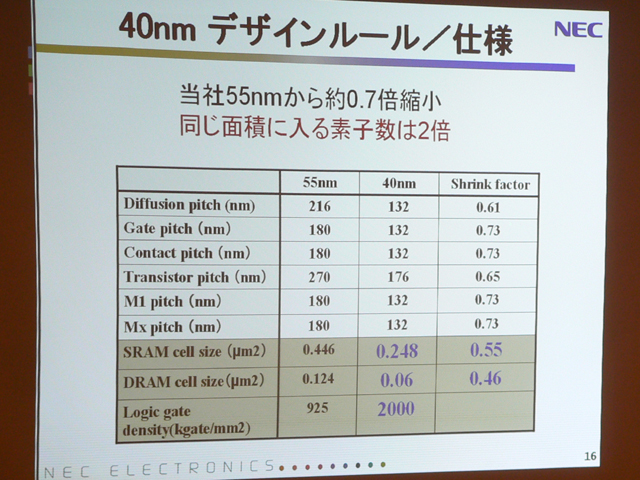
NEC eDRAM

Yeah, the DRAM cell size is similar (maybe rounded up). The TSMC cell size is 0.0583 um^2.

Thought I was actually being useful for once! :mad:
An ieee paper though is a good find though. :)

With a few SIMDs removed (and the DP support nixed), it could be an option. But why not using a Redwood (104mm²)

Indeed. We've had the whole "why base it off rv7xx in the first place"-discussion since we found out about the devkits (rv7xx in 2011). ;)

Perhaps they thought they were being cute with the costs at the time (late 2009).

That is integrated there too, isn't it? Or is it in the CPU chip?
More likely to be the GPU.

alternatively a nominally smaller variant of the R700 series (as a shrunk RV730) to begin with.
I've mentioned a couple thoughts on this awhile back given that rv740 is the only rv7xx @40nm, making it the likely starting base. There was some sort of confirmation (behind the scenes at least) about the early kits using low-clocked 4800 series, which fits if you know that the mobility 4830s were based on rv740.
 
More likely to be the GPU.
That's what I thought, too.
I've mentioned a couple thoughts on this awhile back given that rv740 is the only rv7xx @40nm, making it the likely starting base. There was some sort of confirmation (behind the scenes at least) about the early kits using low-clocked 4800 series, which fits if you know that the mobility 4830s were based on rv740.
As I said, the shader array of RV740 is just a shrink of the RV770's SIMDs to 40nm (with two SIMDs removed) and not a sized up RV730. They obviously didn't change anything compared to RV770 there. They are identical from a functional point of view. So it isn't a real difference to replace one for the other (besides the process and power consumption of course).
 
Well, it's still not trivial moving from 55 ->40nm. The work was long done by late 2009 anyway, so there'd be no point using the 55nm design, especially given the plethora of additions Nintendo asked for (eDRAM, northbridge/ARM etc).

----

(feels like I'm splitting hairs over nothing :oops: Nevermind.)
 
Then, the "slow" ram is not a problem?
I were to post something about function's post because it got me to laugh, I passed because of self discipline to avoid the OT.
As you did, I may answer you that whereas his post has most likely ground in reality, my sarcasmometer went high with a matching laugh, I regret the reputation system that was a damned funny and good post worth "ten points for griffindors" :(
 
That does not make sense as he's talking about 96bit register files. They should be 64bit wide (at least they were), not 32bits in each core.

And a 3D vector would be kind of awkward, as one often needs 4 components anyway (and the size difference of a 3x32bit to a 4x32bit vector unit is probably not huge). If it is not made up, one could have the idea of the support of some reduced precision format (4x24bits) in the same regs, but that does not sound very convincing to me. Other ideas?
Some weird 4x24bit fp SIMD?
I said that already and asked for other ideas. ;)
 
Status
Not open for further replies.
Back
Top