
It's just one person's speculation so far.Anyway back to (~)Larrabee, OK I did not get that Haswell were to use two 8 wide SIMDs.
You are using an out of date browser. It may not display this or other websites correctly.
You should upgrade or use an alternative browser.
You should upgrade or use an alternative browser.
Blazkowicz
Legend
Careful -> only DX10 IGPs (HD3200, Geforce 8200) and later will get you DXVA, flash and browser acceleration.
Looking at your experience, I think you'd be better served with an E-350.
I plan to upgrade to a motherboard with 980G chipset and 4GB ddr3, toy with the iommu and overclock the CPU.
micro-ATX boards with E-350 look great but expensive (can get a low end H61 and sandy bridge pentium for that)
D
Deleted member 13524
Guest
micro-ATX boards with E-350 look great but expensive (can get a low end H61 and sandy bridge pentium for that)
No way, you can find E-350 boards for 95€!
Blazkowicz
Legend
yes but a computer when I can plug only one card is no fun.
It's not a representation of cumulative sales for the last 15 years. It's a representation of the hardware people had in Q1 2011. And the most interesting observation is that a 2005 ultra-low-end IGP is leading the chart...Point being?
I said the list you mentioned represented cumulative sales for the last 15 years. The same list shows the S3 Virge, Intel Extreme Graphics, Ati Rage. My statement stands true.
It's going to take years before the majority of systems will be even capable of running OpenCL reliably at all. And during that time, CPUs won't stop evolving. AVX, AVX2 and eventually AVX-1024 all increase performance/Watt beyond Moore's Law, while GPUs are investing an ever increasing percentage of transistors for programmability and efficiency at ever more complex tasks. So nothing is turning this convergence around.
Put more bluntly; the CPU will continue to be the most reliable source of generic computing power. AMD doesn't stand a chance if it decides to attempt to take a different route. Computing and programmability convergence, Intel's process advantage, and unification of functionality and resource, all favor Intel's move toward a homogeneous architecture.
I'm not forgetting anything. This thread is mainly about Larrabee, desktop CPUs and GPUs, and close derivatives. The ultra-mobile market has different design goals and spending more silicon to achieve the lowest power consumption makes sense for the time being.You're forgetting about the rise of the ARM architecture in tablets, phones and smart/netbooks.
Even ARM is betting on GPU computing, with the OpenCL-oriented Mali 604.
You mean like this: Runescape gameplay on intel gma 950 no lag?This isn't true. Try playing any 3D browser game (runescape, quake live, free realms, fusionfall, etc) and see how your 945G will fare, no matter what CPU you're using.
Intel's current IGPs have become a lot faster since the GMA 950. So they will suffice for many years of casual games to come (and adequately run today's popular hardcore games too).
So really the value of having a more powerful IGP is very limited. Hardcore gamers continue to buy discrete graphics cards so they don't want a Fusion chip, and since future applications will have higher CPU demands too it's not wise to sacrifice CPU performance. Even some games already favor a fast quad-core CPU.
How do APUs help people who upgrade their GPU frequently?I change graphics cards about 3x more than I change CPUs in my desktop.
What huge disparity? Tesla offers ~1 TFLOP theoretical peak performance, but only half that in practice (complex workloads are even worse). It also consumes 200+ Watt and takes 3 billion transistors. Haswell on the other hand is likely to offer 500 GFLOPS at 100 Watt and 1 billion transistors. Granted, NVIDIA will have a new architecture by the 2013 timeframe as well, but it will cost transistors and power to increase efficiency and programmability so I seriously doubt there will be a "huge" disparity. Last but not least, AVX-1024 will give the CPU another performance/Watt advantage to further close the gap, if there will even be a gap left at all...So you disagree with pretty much all of the scientific community related to computing hardware, as you seem to neglect the huge disparity in FLOPS between architectures.
Let's just agree to disagree then.
Getting back to the topic of this thread, what has intel actually said about Haswell and what wrote some journalists speaking with intel about it?
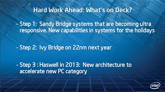
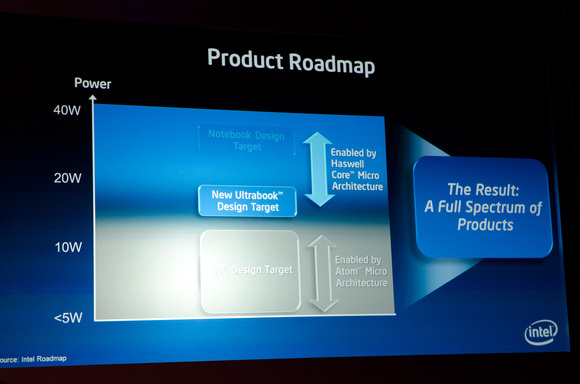
Read that "New architecture to accelerate new PC category"? That refers to that "ultrabook" segment.
Cnet writes:
And heise's Andreas Stiller writes:
"In the beginning of 2013 the 'tock' Haswell is supposed to follow, again designed by the team around Ronak Singhal, which may revive some technologies of the perished Netburst architecture. One hears about a completely new cache design, a relatively short pipeline with 14 stages, new energy saving techniques, and a probably optional vector unit with a width of 512bit speaking LNI: Larrabee New Instructions."
If it comes this way, I would doubt the LNI part a bit. I think of a superset of AVX2, so AVX2-512/1024, maybe with a few additions, is more likely. However, using basically the same instruction set in wide in-order vector units and shallower OoO ones makes it probably quite a bit easier to allocate tasks to the more performant/power efficient ones for each case. And when you can use the same vector units for the integrated graphics as well as from the core side, you wouldn't need to double the computational resources or wouldn't need to write a DX11.x compatible software renderer. Actually that's what Fusion is about, too.
Read that "New architecture to accelerate new PC category"? That refers to that "ultrabook" segment.
Cnet writes:
Does not sound to me like Intel would aim for performance at all costs.Here's what we already know about Haswell, per a conversation I had last month with Intel marketing chief Tom Kilroy: The mobile version of Haswell will be Intel's first system-on-a-chip designed for the mainstream laptop market, according to Kilroy.
And heise's Andreas Stiller writes:
Rough translation:Aber Anfang 2013 soll dann der „Tock“ zum Haswell-Prozessor folgen, der wieder von der Crew in Oregon rund um Ronak Singhal designt wird, die womöglich weitere Techniken aus der untergegangenen Netburst-Architektur wiederbeleben könnte. Man hört zudem von einem komplett neuen Cache-Design, einer vergleichsweise kurzen Pipeline von 14 Stufen, neuen Energiesparmechanismen und einer wahrscheinlich optionalen Vektoreinheit, die mit 512 Bit Breite arbeitet und LNI spricht: Larrabee New Instructions.
"In the beginning of 2013 the 'tock' Haswell is supposed to follow, again designed by the team around Ronak Singhal, which may revive some technologies of the perished Netburst architecture. One hears about a completely new cache design, a relatively short pipeline with 14 stages, new energy saving techniques, and a probably optional vector unit with a width of 512bit speaking LNI: Larrabee New Instructions."
If it comes this way, I would doubt the LNI part a bit. I think of a superset of AVX2, so AVX2-512/1024, maybe with a few additions, is more likely. However, using basically the same instruction set in wide in-order vector units and shallower OoO ones makes it probably quite a bit easier to allocate tasks to the more performant/power efficient ones for each case. And when you can use the same vector units for the integrated graphics as well as from the core side, you wouldn't need to double the computational resources or wouldn't need to write a DX11.x compatible software renderer. Actually that's what Fusion is about, too.
Last edited by a moderator:
ARM has a very, very long way to go to become part of a competitive HPC architecture. It absolutely won't taken Intel longer to implement AVX-1024 than it would take ARM and its partners to gain a foothold in the HPC market.They have all grounds covered but I'm not so sure about them having that much time. ARM cpus may bite into the share sooner than later.
Why? Intel already has quite successful power-efficient 6-core CPUs at 32 nm. An 8-core Haswell capable of delivering 1 TFLOP at the same TDP doesn't seem much of a challenge at 22 nm + FinFET. That would still be a very small chip by today's GPU standards.That's where I get lost. If Intel is really to kill GPUs (whatever their real purpose graphics/compute) they need to deliver more perfs. 8 Haswell cores (or Skylake something) would be big and still far away from GPUs in throughput.
Why are matrix operations an NVIDIA weakness but not for AMD? And what will it cost to reach parity with CPUs?But that is "just" a distinct weakness of Fermi in this respect. They don't handle the matrix operations (which are the base for the top500 list) with very high efficiency. AMD GPUs are actually currently better in this and nvidia promised to improve that considerably with Kepler too (i.e. they aim for parity with CPUs).
Nvidia GPUs lack register space to hold more values in there. So they put more strain on the cache/local memory system (doesn't matter what you use, same [and shared] bandwidth) which is simply a bit too slow. The fastest implementation on AMD GPUs doesn't use the LDS at all (wouldn't have enough bandwidth either), but only rely on the reuse of values in the registers (which have of course enough bandwidth to the units). As AMD GPUs have more registers, the bandwidth of the caches is just fine to reach 90%+ of theoretical peak with large matrix multiplications (as CPUs can also do).Why are matrix operations an NVIDIA weakness but not for AMD? And what will it cost to reach parity with CPUs?
Nvidia has basically two options, increasing register space (if they go to SMs with 64 ALUs, they will probably double registers either way *) and/or increasing bandwidth/size of the shared memory/L1 or a combination of that of course.
*):
Which will only help if they don't need double the amount of threads to fill the units/hide the latencies of course.
Last edited by a moderator:
I never said x86 is the center of the universe. I just think Intel is very close to producing a homogeneous power-efficient high-throughput CPU.I don't believe x86 is the center of the universe. Legacy CPU support isn't a hard requirement in HPC and consumer software may follow suit soon enough.
Why would we come up with new workloads only after CPU-GPU unification? I agree it will allow new workloads which are a complex mix of ILP / TLP / DLP, but I can't really imagine anything beyond that...I agree integration is the future. At least for now. The moment homogenous architectures become good enough we'll come up with new workloads that require dedicated hardware. It's a cycle.
Do you have any supporting arguments? Or are you basing things solely on sentiment?In any case I'm not seeing any indication that AVX will provide competitive performance to discrete GPUs regardless of efficiency advantages. The raw advantage in throughput for GPUs is still too great.
The full support of legacy scalar ISAs and techniques is an albatross when it comes to throughput computing, not a benefit.
GPUs used to have a huge advantage in raw throughput due to exploiting TLP and DLP, while legacy CPUs only exploited ILP. Today's situation is very different. CPUs now feature multiple cores and multiple wide SIMD units, soon to be extended with FMA support. And AVX-1024 gives it the power efficiency of in-order processing. This leaves GPUs with no unique advantages.
Yes, supporting a scalar ISA costs some throughput density, but any APU still requires CPU cores so you have to compare homogeneous architectures against their entire heterogeneous counterpart. Note also that GCN will feature its own scalar ISA...
Why would the thermal and power limits of the CPU socket be any different than those of a graphics card?There's no free pass there. Intel is still constrained by the thermal and power limits of the CPU socket.
What do you mean it did squat? Software renderers which don't use SSE are way slower.Given that AVX is just a wider SSE and the latter did squat for software rendering performance I'm still not seeing reasons to be excited.
I think he means that software renderers that use SSE are still useless for real world gaming.What do you mean it did squat? Software renderers which don't use SSE are way slower.
spacemonkey
Newcomer
Did Intel say anything about the 14nm Skylake and 10nm Skymont?
Let Larrabee RIP
Larrabee is DOA, my friend. Actually, that's a misnomer--it would be more correct to say that Larrabee was stillborn. Actually, it wasn't so much Intel that talked up "real time ray tracing" for Larrabee as it was that wild-eyed 'net pundits, chock-full of Intel hero worship and a deficit of working knowledge about ray tracing, misunderstood some critical things Intel said about Larrabee, and before long all of them were singing the same old Larrabee song, like packs of rabid wolves, howling at the moon! They all went down in flames together the day Intel cancelled Larrabee--forever and a day.
Larrabee was less of a threat to AMD and nVidia than Intel's Sandy Bridge HD x000 IGP is to AMD and nVidia's discrete 3d rasterizers. Even in terms of IGPs, AMD's LLano mops the floor with Intel's SB IGP. I think that AMD is further ahead of Intel in gpu design and manufacture than Intel is ahead of AMD in cpu design and manufacture. But you can forget about Larrabee--it's not going to happen. Please let Larrabee RIP...")
Hi all,
Since Intel's 22 nm FinFET process technology will be production ready at about the same time as TSMC's 28 nm process, I was wondering if this means Intel is actually two generations ahead now.
I think this could give them the opportunity to launch an improved Larrabee product. The inherent inefficiency of such a highly generic architecture at running legacy games could be compensated by the sheer process advantage. Other applications and games could potentially be leaps ahead of those running on existing GPU architectures (e.g. for ray-tracing, to name just one out of thousands).
In particular for consoles this could be revolutionary. They needs lot of flexibility to last for many years, and the software always has to be rewritten from scratch anyway so it can make direct use of Larrabee's capabilities (instead of taking detours through restrictive APIs).
It seems to me that the best way for AMD and NVIDIA to counter this is to create their own fully generic architecture based on a more efficient ISA.
Thoughts?
Nicolas
Larrabee is DOA, my friend. Actually, that's a misnomer--it would be more correct to say that Larrabee was stillborn. Actually, it wasn't so much Intel that talked up "real time ray tracing" for Larrabee as it was that wild-eyed 'net pundits, chock-full of Intel hero worship and a deficit of working knowledge about ray tracing, misunderstood some critical things Intel said about Larrabee, and before long all of them were singing the same old Larrabee song, like packs of rabid wolves, howling at the moon! They all went down in flames together the day Intel cancelled Larrabee--forever and a day.
Larrabee was less of a threat to AMD and nVidia than Intel's Sandy Bridge HD x000 IGP is to AMD and nVidia's discrete 3d rasterizers. Even in terms of IGPs, AMD's LLano mops the floor with Intel's SB IGP. I think that AMD is further ahead of Intel in gpu design and manufacture than Intel is ahead of AMD in cpu design and manufacture. But you can forget about Larrabee--it's not going to happen. Please let Larrabee RIP...
Nick said:Why would we come up with new workloads only after CPU-GPU unification? I agree it will allow new workloads which are a complex mix of ILP / TLP / DLP, but I can't really imagine anything beyond that...
You can't imagine algorithms that require far more raw throughput than is available on current or near future hardware but would benefit from dedicated silicon? I sure hope we're not at the end of the road already!
Do you have any supporting arguments? Or are you basing things solely on sentiment?
I find that question ironic given your unshakeable faith in Intel's ability to upset the status quo with just a few more flops. Where is your supporting evidence that slapping a few vector units onto an x86 CPU will result in computing nirvana or even compete with contemporary GPUs? My opinion is based on the facts on the ground, not wishful thinking.
GPUs used to have a huge advantage in raw throughput due to exploiting TLP and DLP, while legacy CPUs only exploited ILP. Today's situation is very different. CPUs now feature multiple cores and multiple wide SIMD units, soon to be extended with FMA support. And AVX-1024 gives it the power efficiency of in-order processing. This leaves GPUs with no unique advantages.
Sure GPUs have no unique advantages if far higher performance doesn't count as an advantage in your books. Sandy Bridge doubled the FP throughput of Nehalem and it meant nothing for CPU performance in graphics workloads. Why would that change with Haswell?
The Sandy Bridge flagship 2600k has 1/3 of the raw flops of the 550 Ti, the bare minimum required for mid-range gaming. Put Sandy Bridge's shared scheduler to work issuing FP instructions for graphics shaders and texture filtering and let's see how far a "do everything" chip gets.
Yes, supporting a scalar ISA costs some throughput density, but any APU still requires CPU cores so you have to compare homogeneous architectures against their entire heterogeneous counterpart.
Yes, and in that comparison the homogeneous contender is and will be sorely lacking in performance.
Why would the thermal and power limits of the CPU socket be any different than those of a graphics card?
For the same reasons that they're different today. I don't understand your question.
What do you mean it did squat? Software renderers which don't use SSE are way slower.
Why does Ivy Bridge still have an IGP? Software rendering is SLOW. Doubling CPU performance won't change a thing.
A third option would be to increase ILP so they need fewer warps in flight and each of them gets a larger cut of the register file. Simply adopting GF104's superscalar issue could do the trick.Nvidia has basically two options, increasing register space (if they go to SMs with 64 ALUs, they will probably double registers either way *) and/or increasing bandwidth/size of the shared memory/L1 or a combination of that of course.
A third option would be to increase ILP so they need fewer warps in flight and each of them gets a larger cut of the register file. Simply adopting GF104's superscalar issue could do the trick.
If you increase ILP, you'll need more and not less warps in flight.
I beg to differ, at least with regard to the Top500 - I'm aware of some specific MM-Test which show pretty good utilization rates on radeon hardware.But that is "just" a distinct weakness of Fermi in this respect. They don't handle the matrix operations (which are the base for the top500 list) with very high efficiency. AMD GPUs are actually currently better in this and nvidia promised to improve that considerably with Kepler too (i.e. they aim for parity with CPUs). And you always get a better power efficiency when choosing low voltage parts, that is true for GPUs too.
In the Top 500 however, Radeon-based Computers are between 59% efficiency (LOEWE-CSC) and 47% (the first Iteration of Tianhe). The current top-Fermi-cluster reaches 55% and thus does not differ fundamentally. But it sure is a far cry to the efficiency of the top supercomputer which is at 93%.
Yeah, it's worse than 3DMark for games. But I'm sure they'd welcome any advice to improve upon that.The more general problem is actually what the scores tell about the code those computers will actually encounter in reality. It's almost nothing. Just solving huge systems of linear equations isn't what most of these systems do as their daily work.
Throughput will continue to increase, even with a fully homogeneous architecture. What you're claiming is that won't suffice, and we'll get workloads which will require heterogeneous dedicated hardware again. Could you give me an example of a task which requires much more throughput than graphics but less programmability, and would be worth the dedicated silicon?You can't imagine algorithms that require far more raw throughput than is available on current or near future hardware but would benefit from dedicated silicon? I sure hope we're not at the end of the road already!
Compared to SSE, AVX2 increases the throughput fourfold, adds non-destructive instructions, and features gather. That's way more than "just a few more flops", and then some.I find that question ironic given your unshakeable faith in Intel's ability to upset the status quo with just a few more flops. Where is your supporting evidence that slapping a few vector units onto an x86 CPU will result in computing nirvana or even compete with contemporary GPUs? My opinion is based on the facts on the ground, not wishful thinking.
That's sentiment, not fact. GPUs are losing this advantage too. If Sandy Bridge had FMA support and no IGP, it would be less than 200 mm² and deliver 435 GFLOPS. GF116 is 238 mm² and delivers 691 GFLOPS.Sure GPUs have no unique advantages if far higher performance doesn't count as an advantage in your books.
That's merely a 33% advantage in computing density. But let's not forget that a CPU is still a CPU. The GPU is worthless on its own. And the convergence continues...
What's not to understand? You said CPUs are constrained by the thermal and power limits of the CPU socket. So I'm asking, what would keep them from increasing these thermal and power limits?For the same reasons that they're different today. I don't understand your question.
IBM's POWER7 has a 200 Watt TDP, and they fit two of these on a board. And GIGABYTE claims its 24-phase motherboard can deliver up to 1500 Watt to a single socket. Yes it's doubtful that can be sustained, but at least it shows there should be plenty of headroom for high-power CPUs, if there's a market for it. Once homogeneous CPUs replace IGPs and low-end GPUs, they can slowly scale things up when software starts to take advantage of the benefits of software rendering.
Ivy Bridge doesn't have AVX2 nor AVX-1024. IGPs will stay around as long as these haven't been implemented. Software rendering being slow is not a cosmic constant. They're currently limited to using 100 GFLOPS and emulating gather takes 3 uops per element. With four times higher throughput per core, non-destructive instructions, hardware gather, and more cores, software rendering is about to take a quantum leap.Why does Ivy Bridge still have an IGP? Software rendering is SLOW. Doubling CPU performance won't change a thing.
Last edited by a moderator:
That depends on the total memory access latency per warp. CUDA features prefetching, which also benefits from having fewer warps competing for cache space. So increasing ILP with superscalar issue should help in several ways.If you increase ILP, you'll need more and not less warps in flight.
Everything else being equal, more ILP means more warps in flight to hide the same memory latency.That depends on the total memory access latency per warp.
Similar threads
- Replies
- 104
- Views
- 47K
- Replies
- 3
- Views
- 3K