NVIDIA Maxwell Speculation Thread

The question is: does feature level 12_0 exist (and if so what new features will be available) or have we been mislabeling 11_3 as 12_0? My guess is 12_0 still exists (but perhaps not finalized).

From Ryan's article:
It should be noted at this point in time this is not an exhaustive list of all of the new features that we will see, and Microsoft is still working to define a new feature level to go with them (in the interim they will be accessed through cap bits), but ...

So, clearly nothing is finalized at this point. :)
The way the article represents the feature set, features that get released for 12 will also be available in 11. The article never mentions 12_0. Will a client of D3D11 specify a feature level of 12_0 to access all features in 12_0 not surfaced in 11_3? Are all future features surfaced as 11_X, and there is no 12_0? Are 12_Y features specific only to low-level apis, and therefore of no use to D3D11? Is there a bijective mapping between 11_X and 12_Y feature sets? The impression I was left with is that the latter was likely to be the case, but I agree that the situation as described leaves a little much to the imagination....

Also, I don't see how current 11_1 cards could support 11_3 through a software update. 11_3 includes new non-trivial hardware requirements.

I guess it all depends on what current cards have in the way of pre-existing hardware capabilities.
 
Also, I don't see how current 11_1 cards could support 11_3 through a software update. 11_3 includes new non-trivial hardware requirements.
You're assuming all current 11_1 cards features are already exposed in 11_1, which necessarily isn't true (like PRT/Tiled Resources which weren't 'till 11.2)
 
Updated device IDs bring some light:
NVIDIA_DEV.13C0 = "NVIDIA GeForce GTX 980"
NVIDIA_DEV.13C2 = "NVIDIA GeForce GTX 970"

NVIDIA_DEV.13D7 = "NVIDIA GeForce GTX 980M"
NVIDIA_DEV.13D8 = "NVIDIA GeForce GTX 970M"

NVIDIA_DEV.13BD = "NVIDIA Tesla M40"

NVIDIA_DEV.13C1 = "NVIDIA Graphics Device "
NVIDIA_DEV.13C3 = "NVIDIA Graphics Device "
http://forums.laptopvideo2go.com/topic/31126-inf-v5014/
http://forums.laptopvideo2go.com/topic/31117-inf-v5013/
http://forums.laptopvideo2go.com/topic/31065-inf-v5011/

So M40 seem to be GM204 based, 1:32 DP would be a bit low for this name. Maybe its just crippled on GeForce like on 780/780 Ti at 1/8 and Tesla GM204 has 1:4.
Maybe the other 13Cx Device will be GTX 970 Ti and GTX 960.
 
It's not the ROPs. Each SMM can output 16 bytes (4x32b pixels) per clock. 970 only has 13 SMM's ==> 13x4 = 52.
There seems to be a bit more going on. If you look at the blending results (other than plain 4x8bit) there's still lots of difference between GTX 980 and 970, even for things which are slow-as-molasses like 4xfp32 blend, which should not be limited by SMM export at all.
 
You're assuming all current 11_1 cards features are already exposed in 11_1, which necessarily isn't true (like PRT/Tiled Resources which weren't 'till 11.2)

We knew PRT was available at GCN's launch (obviously wasn't in D3D at launch). I doubt they've been hiding big features like conservative rasterization/etc. for this long. ;)
 
00-power-consumption-r2kct.png


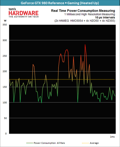
Nvidia's newest architecture presents us with a whole new set of challenges for measuring power consumption. If the maximum of all four possible rails are to be measured exactly (to find out Maxwell’s power consumption reduction secrets), then a total of eight analog oscilloscope channels are needed. This is because voltage and current need to be recorded concurrently at each rail in real-time. If the voltages are measured and then used later, the result may be inaccurate. So, how did we solve this problem?

We enlisted the help of HAMEG (Rohde & Schwarz) to search for a solution with us. In the end, we had to use two oscilloscopes in parallel (a master-slave triggered setup), allowing us to accurately measure and record a total of eight voltages or currents at the same time with a temporal resolution down to the microsecond.


To illustrate, let’s take a look at how Maxwell behaves in the space of just 1 ms. Its power consumption jumps up and down repeatedly within this time frame, hitting a minimum of 100 W and a maximum of 290 W. Even though the average power consumption is only 176 W, the GPU draws almost 300 W when it's necessary. Above that, the GPU slows down.

More details here
http://www.tomshardware.com/reviews/nvidia-geforce-gtx-980-970-maxwell,3941-11.html
 
If the chip doesn't maintain above TDP power draw for periods that measure more than a few milliseconds, if none of the transient spikes exceed the maximum power rating (not the same thing as TDP), if the chip's local temperatures don't climb past ~100-120 C, and none of the packaging and silicon-level physical limits are exeeded, the oscilloscopes are nothing but irrelevant nitpicking at the rate of millions of times a second.
The amount we need to care about this is proportional to the measurement granularity.

If there is sustained draw above TDP, or regularly measured spikes that exceed the safe bounds listed for the chip or power delivery circuitry, it might be worth the bandwidth used to read the page.
I see no sign of that kind of analysis, and they might be interested in seeing how everything that has come before it has behaviors that show up with high-speed oscilloscopes.
 
If [...] the oscilloscopes are nothing but irrelevant nitpicking at the rate of millions of times a second.
Agreed, although I don't fully understand what causes these spikes in the first place. Obviously some parts of a frame will be much more power-hungry than others but it's strange to see a spike at 275W+ for what's presumably nowhere near a true power virus. Is there some buffering going on? (i.e. capacitors in electrical terms I guess :p)
 
Agreed, although I don't fully understand what causes these spikes in the first place. Obviously some parts of a frame will be more power-hungry than others but it's strange to see a spike at 275W+. Is there some buffering going on? (i.e. capacitors in electrical terms I guess :p)

Possibly things like high utilization where a lot of SIMD units switch at the same time, current inrush from a ton of clock-gated units waking up, a confluence of high ALU activity, high memory bank and memory bus utilization, all this happening right after the heuristic for turbo determined it had enough margin to ratchet voltage and clock, bad luck, etc.

Sandy Bridge added hundreds of cycles in waking up to full AVX-256 mode, likely related to the sudden power demand of hundreds of thousands to millions of transistors that had close to no impact on the power delivery grid now requiring power to reach their active states and perform work.

Waking up power-gated cores is a pretty intensive endeavor as well, what with the capacitance of hundreds of millions of transistors and billions of wires that were effectively zero one instant and now a cascade of activity and short circuits if it weren't until the very long (in cycle terms) graduated wakeup process.


It's a question of how much of the chip is twitching in a given time period and what the electrical delivery system is primed to do right then and there, and this is something that a number of measures like dynamic gating, voltage and clock adjustment, and circuit tuning to minimize the number of transistors that are active in the common case (until you hit a pathological input) can make worse in the uncommon worst case.

There is more than enough hardware and wires than necessary to melt the chip down several times over.

edit: And I forgot about the changing physical and electrical properties of highly variable silicon that can heat up dozens of degrees in microseconds in a system that is perpetually teasing with thermal runaway.
 
Is there some buffering going on? (i.e. capacitors in electrical terms I guess :p)

Does the article cover power factor at all? Is voltage stable and only current varying? At the end of the day, are you measuring the system, or the card? I'm a poor programmer, analog circuits frighten and confuse me :>

The spike seem less interesting than the shift under load, and both of those seem not as unlikely as the factor of two difference in idle power consumption....
 
We knew PRT was available at GCN's launch (obviously wasn't in D3D at launch). I doubt they've been hiding big features like conservative rasterization/etc. for this long. ;)

That's why I specifically mentioned "all" there, as for example Tonga is still somewhat unknown thing, no-one has figured out where those 700 million transistors + 128bit mem controllers worth of transistors went if the currently known specs are what it is
 
current inrush from a ton of clock-gated units waking up [...]Waking up power-gated cores is a pretty intensive endeavor as well,
Just making sure I understand this correctly - you're saying that both clock gating and power gating would result in a (short) higher peak when resuming after being turned off than the actual power consumption of the units when continuously turned on?

i.e. in the pathological case of the exact same design having *no* power/clock gating whatsoever, the average power consumption would be massively higher, but the peak power consumption over an extremely short amount of time might be significantly *lower*? I do remember reading up some about that but I never thought about it much...

all this happening right after the heuristic for turbo determined it had enough margin to ratchet voltage and clock
Good point. It still annoys me a bit that there's no way to disable turbo (even if it means always being at base clock!) for performance analysis purposes.

There is more than enough hardware and wires than necessary to melt the chip down several times over.
Tsk tsk, don't tell that to people who make a big deal out of chips exceeding their TDPs without thermal/power throttling ;) I agree the simple reality is there's no way to guarantee a TDP without losing the *majority* of your performance or supporting some form of throttling. The only decision is how much you value performance stability versus throttling in real-world applications... (see e.g. iOS vs Android devices).
 
Just making sure I understand this correctly - you're saying that both clock gating and power gating would result in a (short) higher peak when resuming after being turned off than the actual power consumption of the units when continuously turned on?
There's an instantaneous power cost to wakeup, especially for power gating. Power gates themselves have a power cost when they switch, especially since they need to be physically larger than most gates to keep their leakage low and to offer a low-resistance path to the power that the rest of the unit/core relies on when on.
The big thing for power gating something the size of a core is that all the power delivery, clocking, local sources of decoupling capacitance, and other devices in the off region need to be charged, and without a graduated process there's a lot more metal and silicon that was set to ground that needs to be raised. It can without protective measures exceed the overal SOC's ability to supply current without damage or compromising the stability of the rest of the actively operating chip.
Because this infrastructure is expected to be highly available and capable of handling very high peak demand (multiple high-demand units), it is physically able to draw that much power and it is at least possible to do so much more quickly than any single unit would need.
If we're operating with designs that are vastly overprovisioned in peak power demand relative to the average case, we already know it's quite possible that there's already active hardware eating up most of the budget right when the gated areas need to wake up.
There are various measures, like integrated VRMs, or AMD's adaptive clocking that seek to reduce the time it takes to react to big electrical events or make the circuitry able to to slow itself long enough to wait them out without compromising functionality.

Clock gating can be mild enough, particularly for already complex clocking schemes, so the most advanced versions of it like Intel's can happen at a cycle or near cycle granularity without being a net negative. For less-advanced versions, I'm not sure that's always true.
The perverse outcome for power-saving is, particularly for highly parallel hardware, that lowering the average consumption means the designer no longer has to say "nope, I can't add these extra units because average consumption would be too high".
Sizing the design so that its likely workloads usually won't exceed the power budget allows for a higher peak when they do.

i.e. in the pathological case of the exact same design having *no* power/clock gating whatsoever, the average power consumption would be massively higher, but the peak power consumption over an extremely short amount of time might be significantly *lower*? I do remember reading up some about that but I never thought about it much...
Without power and clock gating, the design is likely to be smaller. However, without guarantees as to what it might do in a pathological case, it might be smaller unless we provision for a throttle or fail-safe, otherwise it might be kept smaller or slower out of fear of a transient event that could damage it.
Everything else being equal, on a sustained basis the stripped-down design is likely to have a lower peak power (less controller hardware, less complexity for power delivery, fewer big gates, no wakeup penalties) in a perfectly loaded scenario, but it would be massively less efficient everywhere else and in reality would probably need to be more conservatively designed and have more conservative clocks and voltages.

A design with those measures is more complex, and there's a power cost to the extra control hardware, the monitoring hardware, extra widgets now sitting in the clock tree or the power delivery circuitry, and there are various penalties related to wakeup that need to be compensated for through either judicious use of gating or being able to eat into the guard bands that a more primitive design has to leave in place, leading to more variability in clocks and voltages.
The design now tries to leave as much of the chip as quiescent as possible, but for the sake of performance allows them to wake up, incur startup costs, do so when the chip is not in a low-voltage or low-clock step, and all while the rest of the chip is already under heavy load and much hotter than at cold boot.

Tsk tsk, don't tell that to people who make a big deal out of chips exceeding their TDPs without thermal/power throttling ;) I agree the simple reality is there's no way to guarantee a TDP without losing the *majority* of your performance or supporting some form of throttling. The only decision is how much you value performance stability versus throttling in real-world applications... (see e.g. iOS vs Android devices).
The thing is, particularly for the oscilloscope measurements, is that allowing for above TDP transients has been a thing probably since people though to set down standards for putting metal blobs on top of their CPUs. I don't get at this point what Tomshardware's setup does that isn't like pointing out that cars on a highway with a low speed limit have speedometers that go much higher.
It was physically impractical or electrically intractable to prevent any and all above TDP transients decades ago, and barring extremely low-power and super-simple devices for implantable chips or the simplest of wearables, it may not be physically possible.

If they try to turn that setup on older chips, imagine how far back they'll find that Santa was just their parents putting presents under the tree.
 
I wouldn't call a 240W average over a 60 second period a transient spike, though ;-). At least I assume the measurements were done properly, the equipment certainly looks expensive enough :).
 
You don't need a high-speed oscilloscope if the power draw averaged over a few milliseconds is above TDP.
It's a specification that adjusts for the way a cooler's physical bulk will smear together energy outputs that on a fine scale can be very erratic.
The idea is that it's pointless and unreasonable to expect a thermal solution to worry about such things, and it more than averages out at human time scales.
 
If the chip doesn't maintain above TDP power draw for periods that measure more than a few milliseconds, if none of the transient spikes exceed the maximum power rating (not the same thing as TDP), if the chip's local temperatures don't climb past ~100-120 C, and none of the packaging and silicon-level physical limits are exeeded, the oscilloscopes are nothing but irrelevant nitpicking at the rate of millions of times a second.
The amount we need to care about this is proportional to the measurement granularity.

If there is sustained draw above TDP, or regularly measured spikes that exceed the safe bounds listed for the chip or power delivery circuitry, it might be worth the bandwidth used to read the page.
I see no sign of that kind of analysis, and they might be interested in seeing how everything that has come before it has behaviors that show up with high-speed oscilloscopes.

We certainly don't need to care about this as consumers, but it sure is interesting.

In particular, I wonder if previous GPUs exhibited this much variance within a single millisecond, and if not, whether that might be one of the keys to Maxwell's power efficiency. Or perhaps I should say energy efficiency.
 
Back
Top