
Luminescent
Veteran
R300:
sireric said:The real die and real area would never be given out.
")
Dave H said:....Nvidia can probably be properly accused of hubris in thinking that they could tailor their product to address a new and rather different market segment (low-end production rendering) while still maintaining product superiority in the consumer market. Or of arrogance in assuming they were the only IHV worth paying attention to, and thus could influence future specs to reflect their new architecture instead of one that better targeted realtime performance.
Obviously one can correctly accuse their marketing of all sorts of nasty things.
But I don't think one can really accuse Nvidia of incompetence, or stupidity, or laziness, or whatnot. NV3x is not really a bad design. It's unquestionably a decent design when it comes to performance on DX7 and DX8 workloads. I can't entirely judge, but I would guess it's about as good as could be expected in this timeframe as an attempt to replace offline rendering in the low-end of video production; I just don't think that's quite good enough yet to actually capture any real part of the market.
The only thing it's truly bad at is rendering simple DX9-style workloads (and yes, HL2 is very much on the simple end of the possibilities DX9 represents) at realtime interactive framerates. And--except with the benefit of hindsight--it doesn't seem obvious to me that Nvidia should have expected any serious use of DX9 workloads in the games of the NV3x timeframe. This prediction turns out to have been very, very wrong. (What I mean by "the NV3x timeframe" does not end when NV40 ships, but rather around a year after NV3x derivatives are dropped from the mainstream of Nvidia's product lineup. After all, the average consumer buying a discrete video card expects it to hold up decently for at least a while after his purchase.)
It turns out that DX9 gaming is arriving as a major force quite a bit ahead of DX9 special effects production. And Nvidia will rightly pay for betting the opposite. But, viewed in the context of such a bet, their design decisions don't seem that nonsensical after all.
Perhaps what you mean is that their hardware is so slow at handling "DX9 special effects" that "DX9 special effects production" work is all it's good for? I find this a pretty nonsensical idea....I *hope* this is not what nVidia was thinking...Very interesting point about from-scratch vs. evolutionary designs. Getting back to the original issue: do you think the decision to base DX9 around FP24 was sealed (or was at least evident) early enough for Nvidia to have redesigned the NV3x fragment pipeline accordingly without taking a hit to their release schedule? (And of course the NV30 was realistically planned for fall '02 before TSMC's process problems.) Obviously a great deal of a GPU design has to wait on the details of the API specs, but isn't the pipeline precision too fundamental to the overall design? Or is it?sireric said:In general, a from-scratch design takes on the order of 3 years from architecture spec to production. However, GF's have never had a from scratch design that I can see. Evolutionary instead (which is not bad -- don't get me wrong; it has pros & cons). Consequently, the design cycle is probably shorter. Both ATI & NV had plenty of input into DX9, as well as a good (not great) amount of time to incorporate needed changes.
Right. To be clear, I wasn't claiming that computation precision affected the required per-pixel bandwidth. Rather that your available bandwidth requires a certain level of fillrate to balance it, and that your transistor budget would then put limitations on the precision at which you achieve that fillrate. The question is how large a factor the ALUs really are in the overall transistor budget--whether a ~2.5x increase in ALU size (from FP24->FP32) is enough to warrant cutting down on the number of pixel pipes or the computational resources in each pipe.Lots of stuff in there. The computation / bandwidth ratio is interesting, but I'm not sure it makes that much sense. The raw pixel BW required is not determined by the format of your internal computation engine, but more about the actual surface requirements per pixel.
...and apparently the answer is no. Which brings the mind the question of why Nvidia stuck with a 4x2 for NV30 and NV35, if not because they didn't have the transistor budget to do an 8x1. Two ideas spring to mind. First, that they were so enamored of the fact that they could share functionality between an FP32 PS 2.0 ALU and two texture-coordinate calculators that they went with an nx2 architecture. Second, that they planned to stick with a 128-bit wide DRAM bus after all; that NV35 is not "what NV30 was supposed to have been", but rather the quickest way to retrofit improved performance (particularly for MSAA) onto the NV30 core; and that if NV35's design seems a little starved for computational resources compared to its impressive bandwidth capabilities (particularly w.r.t. PS 2.0 workloads), that's because it was just the best they could do on short notice.Honestly, the area increase from 24b to 32b would not cause you to go from 8 to 4 pixels -- It would increase your overall die cost, but not *that* much. It's just a question of would it justify the cost increase? For today, it doesn't.
Hmm. I don't recall seeing too many real-world examples over a factor of ~3x (hence 65% behind). FWIW I'm talking about benchmarks of real games that might ship in the next, say, year or less: something like HL2 (or even a *bit* more shader-intensive) at 1600*1200, running an in-game workload. Perhaps if you're talking performance (maybe clock-normalized?) on straight synthetic shaders you might get to ~5x. Or are you suggesting there's even worse to come?Actually, the performance difference appears to be 2~5x, when running complexe shaders. It's not just register usage (though that's a big one).(If NV3x chips, like R3x0, could use all the registers provided for by the PS 2.0 spec without suffering a performance penalty, their comparitive deficit in calculation resources would still likely leave them ~15-25% behind comparable ATI cards in PS 2.0 performance. But that is nothing like the 40-65% we're seeing now.)
Well there goes that theory. I do wonder where I've gotten that impression about R3x0 and multiple levels of texture dependancy (it was second-hand, of course), but obviously you're the authority on this one.BS. The R300 has no performance hit at 1,2 and sometimes a slight performance when hitting 3 and 4 levels of dependancy. The performance hit an NV3x gets in just defining 4 temporaries is much larger than the R3x0 gets in doing 4 levels of dependancies. The worst 4 levels perf hit I've ever seen is in the 10~15% range. The R3x0 is VERY good at hiding latencies.Where R3x0 and NV3x come into this is in performance for dependent texture reads. I'd be interested in having more specifics, but as I understand it the R3x0 pipeline is deep enough to do an alright job minimizing the latency from one level of dependent texture reads (particularly if you fetch the texture as much in advance of when you need it as possible), but woe be unto you if you're looking for two or three levels. Meanwhile, NV3x is reputed to do just fine mixing several levels of texture reads in to the normal instruction flow--meaning that it must do a gangbusters job at hiding latency. Meaning it has a hell of a deep pipeline.
Yeah, gee, Walt, only a big fucking idiot would think that.WaltC said:I think your idea of "DX9 special effects production" is pretty funny--I mean, that you'd think that...
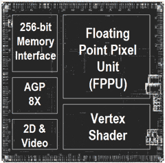
sireric said:That image has a little bit of.... "Marketing" thrown into it. The real die and real area would never be given out. The image is more conceptual in nature, then reflecting the real area of things. Sorry.
Dave H said:Yeah, gee, Walt, only a big fucking idiot would think that.WaltC said:I think your idea of "DX9 special effects production" is pretty funny--I mean, that you'd think that...
zurich said:I think Dave H's points are well articulated. Unlike the GF 1/2/3/4, the GFFX looks like a workstation card turned into a gaming card, instead of vice versa. It'd make sense that it was geared towards DX9 content creation, rather than actually DX 9 gaming. I mean, the pick up rate for DX8 was pretty pathetic.
WaltC said:Dave H said:Yeah, gee, Walt, only a big fucking idiot would think that.WaltC said:I think your idea of "DX9 special effects production" is pretty funny--I mean, that you'd think that...
Dave, this trend is the same trend that's been going on for years and years. What it might have to do with nV3x and DX9, in particular, and apart from any other 3D chip and windows API ever made, I can't imagine.
Dave H said:Very interesting point about from-scratch vs. evolutionary designs. Getting back to the original issue: do you think the decision to base DX9 around FP24 was sealed (or was at least evident) early enough for Nvidia to have redesigned the NV3x fragment pipeline accordingly without taking a hit to their release schedule? (And of course the NV30 was realistically planned for fall '02 before TSMC's process problems.) Obviously a great deal of a GPU design has to wait on the details of the API specs, but isn't the pipeline precision too fundamental to the overall design? Or is it?
No, it wasn't. I don't think FP32 would of made things much harder, but it would of cost us more, from a die cost.Or, since you might not be able to speak to Nvidia's design process: was R3x0 already an FP24 design at the point MS made the decision? If they'd gone another way--requiring FP32 as the default precision, say--do you think it would have caused a significant hit to R3x0's release schedule? Or if they'd done something like included a fully fledged int datatype, would it have been worth ATI's while to redesign to incorporate it?
...and apparently the answer is no. Which brings the mind the question of why Nvidia stuck with a 4x2 for NV30 and NV35, if not because they didn't have the transistor budget to do an 8x1. Two ideas spring to mind. First, that they were so enamored of the fact that they could share functionality between an FP32 PS 2.0 ALU and two texture-coordinate calculators that they went with an nx2 architecture. Second, that they planned to stick with a 128-bit wide DRAM bus after all; that NV35 is not "what NV30 was supposed to have been", but rather the quickest way to retrofit improved performance (particularly for MSAA) onto the NV30 core; and that if NV35's design seems a little starved for computational resources compared to its impressive bandwidth capabilities (particularly w.r.t. PS 2.0 workloads), that's because it was just the best they could do on short notice.
Well, 3x would be 33% in my book. I don't remember the shadermark results, but I thought some were more than 3x. Our renderman conversion examples (using Ashli to generate DX9 assembly) showed up to 5x using some sort of 4x driver set from NV.Hmm. I don't recall seeing too many real-world examples over a factor of ~3x (hence 65% behind). FWIW I'm talking about benchmarks of real games that might ship in the next, say, year or less: something like HL2 (or even a *bit* more shader-intensive) at 1600*1200, running an in-game workload. Perhaps if you're talking performance (maybe clock-normalized?) on straight synthetic shaders you might get to ~5x. Or are you suggesting there's even worse to come?
Well there goes that theory. I do wonder where I've gotten that impression about R3x0 and multiple levels of texture dependancy (it was second-hand, of course), but obviously you're the authority on this one.
Not sure I'll get an answer on this but...so what do you think? I mean you must have some good ideas about what's causing the severe register pressure on NV3x. Surely Nvidia would love to offer more than 2 full-speed FP32 registers if they could. Is it a result of some other feature of the NV3x pipeline (static branching, say, although I'm not sure why this would be the case)? Or perhaps some likely piece of broken functionality that wouldn't have had time to be fixed for NV35?
Any thoughts would be appreciated...
Dave H said:Maybe you should try reading the linked post, then.
(And incidentally, obviously such work would be done in OpenGL and not DX9, but it's the featureset of FP calculations and reasonably flexible vertex and fragment shaders that DX9, ARB_fragment_program, NV_fragment_program etc. expose that's being discussed here.)
John Carmack said:...The current generation of cards do not have the necessary flexibility, but cards released before the end of the year will be able to do floating point calculations, which is the last gating factor....
I'm really not sure that's an accurate depiction. As far as I can tell, from the evidence posted in the thread you linked earlier, the R300 need only have a multiplier and an adder in serial to have the performance characteristics supplied (making for one MAD per clock), not one MAD, and one unit capable of doing a few other things.DaveBaumann said:Eh? As far as we know so far NV35 has a full combined ALU & texture address processor and two smaller ALU's for each of its 4 pipes. R300, ignoring the Vec/Scalar coissue, has an FP texture address processor a full ALU and a small ALU for each of its 8 pipes. Thats 12 FP processors for NV35 and 16 for R300, excluding the texture address processor, 24 including.
The point is that it's capable of full precision. While I'm not sure how it stacks up against 3DLabs' own solution right now, it is a definite step ahead of the R3xx in precision, which may make it the only current viable solution for low-end offline rendering.WaltC said:Right, it's not just DX9 that's slow at full precision on nV3x, it's ARB2, as well.
The point for me is that the idea that nV3x was designed for "workstations" and not "3d gaming" is simply void, as it suffers from the same problems in workstation useage--it's slow at full precision there, too.
Chalnoth said:I'm really not sure that's an accurate depiction. As far as I can tell, from the evidence posted in the thread you linked earlier, the R300 need only have a multiplier and an adder in serial to have the performance characteristics supplied (making for one MAD per clock), not one MAD, and one unit capable of doing a few other things.