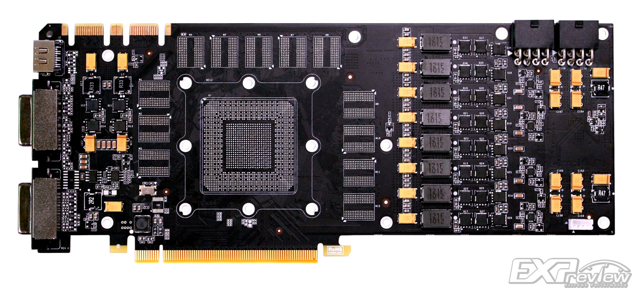
Some hynix 2gbit ddr3 chip (mentioned in the "graphic card memory" category) is 13.0x9.0mm. Can't tell you though if they have standardized physical dimensions.Hmm, I can't "lock" on any reference measure in this one. Anyone have the dimensions of those DDR3 chips?
edit: with that ddr3 chip size I get about 130-140mm² for gk107, so slightly bigger than CV.
Last edited by a moderator:
")