
You are using an out of date browser. It may not display this or other websites correctly.
You should upgrade or use an alternative browser.
You should upgrade or use an alternative browser.
PowerVR Series 6 now official
- Thread starter roninja
- Start date
http://www.acrofan.com/ko-kr/commer...12&ucode=0001030001&page=1&keyfield=&keyword=
4 taped out
2 in silicon
4 taped out
2 in silicon
G6230 / 430 announced.
Colour me confused: http://imgtec.com/News/Release/index.asp?NewsID=686
G6200 = 2 clustersFollowing on from the G6200 and G6400 cores, the PowerVR G6230 and G6430 offer two further design points in the Series6 family, which now includes two ‘two-cluster’ and two ‘four-cluster’ IP cores.
G6230 = 2 clusters
G6400 = 4 clusters
G6430 = 4 clusters
***edit: brainfarts removed.
ltcommander.data
Regular
http://www.imgtec.com/News/Release/index.asp?NewsID=686G6230 / 430 announced.
So how are the G6x30 series different? When they say "extra area for maximum performance" do they mean each cluster gets more pipelines/EUs? Or are the G6x30 series the DX11.1 parts vs the regular DX10, where "performance" is less about raw performance than more advanced features enabling efficiencies?PowerVR G6200 and G6400 are designed to deliver the best performance at the smallest area possible for two and four cluster architectures respectively, while the PowerVR G6230 and G6430 ‘go all out’, adding incremental extra area for maximum performance whilst minimising power consumption.
EDIT: Didn't originally see Ailuros's post. So does the G6x30 series mean MP configurations rather than internally beefed up clusters? I read "two ‘four-cluster’ IP cores" as there are now 2 four-cluster designs ie. G6400 and G6430, but I can see it meaning an MP config as well.
Last edited by a moderator:
Hmmm the G6x30 parts being DX11.1 would be a reasonable theory I didn't think of.
If marketing didn't just copy the following paragraph from a past announcement:
By the way the acrofan link has an interesting Rogue block diagram:
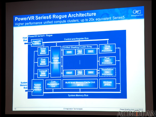
The tesselation engine block looks like optional the way its been displayed.
One more thing: it seems that two USC blocks have a "shared texture pipeline" at a time. 1 quad TMU shared between two shader clusters?
If marketing didn't just copy the following paragraph from a past announcement:
and the highlighted part means that even G6430 isn't surpassing the 1 TFLOP range, then it might make sense.PowerVR Series6 GPU cores are designed to offer computing performance exceeding 100GFLOPS (gigaFLOPS) and reaching the TFLOPS (teraFLOPS) range enabling high-level graphics performance from mobile through to high-end compute and graphics solutions.
By the way the acrofan link has an interesting Rogue block diagram:
The tesselation engine block looks like optional the way its been displayed.
One more thing: it seems that two USC blocks have a "shared texture pipeline" at a time. 1 quad TMU shared between two shader clusters?
Dominik D
Regular
Good luck for me or anyone else outside IMG finding the difference between a GC6230 and a GC6400 for instance.
If you Google Translate this:
http://www.acrofan.com/ko-kr/commer...cate=0103&wd=20120612&ucode=0001030001&page=1
You get:
"(...) PowerVR Series 6 GPU PowerVR G6230 and G6430 GPU IP (...) was optimized [for] power consumption performance compared to existing PowerVR G6200, G6400 (...) [reinforcing] high computation efficiency while delivering the power and is characterized by minimal bandwidth requirements."
Whether this is the case or not - I wouldn't know.
I have no idea how you're getting that from the quoted part. :|G6200 = 2 clusters
G6230 = 2*(2 clusters)
G6400 = 4 clusters
G6430 = 2*(4 clusters)
ltcommander.data
Regular
But fatter in the SGX530 vs SGX540 sense where each cluster has more EUs or fatter in the Series 5 vs Series 5XT sense where each EU has been redesigned and beefed up?The G6230 and G6430 seem like just higher performance tuned variants (fatter) of the original two and four cluster cores, not the DirectX 11.1 compliant cores or MP configs or anything else (though the logic to glue to MP solutions is likely baked in there from the start).
But fatter in the SGX530 vs SGX540 sense where each cluster has more EUs or fatter in the Series 5 vs Series 5XT sense where each EU has been redesigned and beefed up?
Is fatter in the sense of having design optimizations trading area for attainable clock speed an option too?
But fatter in the SGX530 vs SGX540 sense where each cluster has more EUs or fatter in the Series 5 vs Series 5XT sense where each EU has been redesigned and beefed up?
If you're willing to call ALUs = clusters in Series5 then you have:
530 = 2Vec2, 1 TMU
540 = 4Vec2, 2 TMUs
...in other words under that reasoning and since Series5 cores have in their majority a 2:1 ALU/TMU ratio, the 540 is basically a "2 cluster" 530 oversimplified. Exception is the 535 with a 1:1 and the 554 with a 4:1 ALU/TMU ratio.
Series5XT most significant change IMO was that the cores where multicore capable and since it's obviously not a sw based solution it sounds to me like the bigger investment in R&D. Dual issue for the ALUs doesn't sound as complicated compared to the first but that's just me. It should be cheaper in hw then adding twice the ALU amount, yet the obvious tradeoff could be that you don't get automatically twice the arithmetic efficiency under all cases.
Now Rogue bites into another field; I'd be VERY surprised if any of the next generation small form factor GPUs still has vector ALUs, meaning that things on multiple fronts aren't as easily comparable to the current generation of GPUs. First of all I'd suggest that Rogue will have a much higher ALU:TMU ratio than Series5 and 5XT cores; it should be either equal or higher to that of a SGX554.
So on a purely speculative level (and yes I'm sure I'm wrong again) it could be something like:
SGX554 = 4 Vec4 <-> 2 TMUs <-> 4 Vec4
G6200 = 5 SIMD16 <-> 4 TMUs <-> 5 SIMD16
In the 2nd case either going dual issue or more SIMDs sounds like overkill to me given the resulting ALU/TMU ratio, but that's just me. Besides they haven't even rolled out yet the first batch of Rogue cores and any design refreshes would take far more time then I assume lies in between 6x00 and 6x30 cores. If IMG senses down the line that any competitor has a higher arithmetic throughput it might be an idea, but my gut feeling tells me that Rogue doesn't have to worry much for quite some time to come. If IMG would have to worry about anything then it would be their partners' integration/execution timetables.
DX10.1 vs. DX11.1 sounds likelier as it stands and yes again all IMHO.
Is fatter in the sense of having design optimizations trading area for attainable clock speed an option too?
It should be definitely also the case; in a contrary case we wouldn't talk about a new GPU generation targeted at 28nm at least as a starting point IMO. When Series5 was announced performance figures had been quoted under 90nm with a frequency of 200MHz.
Now Rogue bites into another field; I'd be VERY surprised if any of the next generation small form factor GPUs still has vector ALUs, meaning that things on multiple fronts aren't as easily comparable to the current generation of GPUs. First of all I'd suggest that Rogue will have a much higher ALU:TMU ratio than Series5 and 5XT cores; it should be either equal or higher to that of a SGX554.
Are you saying that you expect a transition from explicit parallelism to implicit/threaded parallelism, like what nVidia introduced with G80?
Unless I'm missing something, Series 5XT achieves parallelism in the following fashions:
1) By allowing two FP16 or three/four Fixed8/10 operations where normally one 32-bit operation would be allowed.
2) By allowing two 32-bit operations to be performed while an operand is shared between them.
3) Co-issue allowing two instructions to be performed simultaneously.
The first two at least are a pretty obvious optimization of register file space/access ports and execution resources, for when you don't need full precision. And specifying lower precision in shaders is a heavily advised optimization strategy for IMG's GPUs. All three of these techniques seem to require explicit parallelism, where it's lost with a SIMT approach. I could see adding SIMT on top of this scheme, but why would they abandon these existing techniques, outside of co-issue perhaps?
I obviously can't answer those questions without possibly making a complete fool of myself. However my gut feeling is supported by the various tidbits/hints I can read left and right like this one:
http://withimagination.imgtec.com/
Another very important aspect of Power VR Series6’s GPU compute capabilities lies in how the graphics core can dramatically improve the overall system performance by offloading the CPU. The new family of GPUs offers a multi-tasking, multi-threaded engine with maximal utilization via a scalar/wide SIMD execution model for maximal compute efficiency and ensures true scalability in performance, as the industry is sending a clear message that the CPU-GPU relationship is no longer based on a master-slave model but on a peer-to-peer communication mechanism.
FY 12 presentation: http://www.imgtec.com/corporate/presentations/prelims12/index.asp
Nothing particular new, except that they went from 245M units 2010/1 to 325M for 2011/2.
Nothing particular new, except that they went from 245M units 2010/1 to 325M for 2011/2.
FY 12 presentation: http://www.imgtec.com/corporate/presentations/prelims12/index.asp
Nothing particular new, except that they went from 245M units 2010/1 to 325M for 2011/2.
They also said(either in that document or in the audio) "around" 10 rogue licencees and "around" 20 rogue Socs in development.
They also said(either in that document or in the audio) "around" 10 rogue licencees and "around" 20 rogue Socs in development.
The presentation states "approaching 20 SoCs" for Rogue. So let's cut the bargain at 9/18 for now

At least now we know what Alex looks like
Similar threads
- Replies
- 18
- Views
- 7K
- Replies
- 89
- Views
- 32K
D
- Replies
- 3
- Views
- 3K