Semi Accurate's 4XX views

Status
Not open for further replies.
Its not really deeper in the pipeline, both architectures are similar in that regard, its just that nV has more tessellation (polymorph) units. But over all, you still need serious amounts of shader power to do tessellation and displacement.

GF100small.png

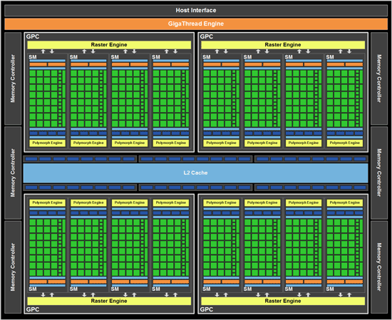
From the block diagram u can see that a single polymorph engine has only 32 SP-s aviable max. Cant do anything else with the others. So the whole tesselation pipeline Hull shader, Tesselator, Domain shader (so the displacement too) is running on the same 32 SP-s. Just paralel with the other 15. At least thats what i see from the diagram. :rolleyes: Maybe they can keep track of each other trough the L2 cache but cant help each other directly.

Right now even a 2 GPC and 8 polymorph card would be miles ahead of cypress in tesselation. But that could change with the next radeons.
 
The polymorph engine is only the tessellator in the first stage all other portions of tessellation and displacement take place in the shader units. The data is sent to the hull shader which tells the domain and geometry shader where the placement of the new vertexes should be and the respective shaders will calculate position based on this information. With adaptive tessellation the geometry shader can do this on the fly.

After all this the data is sent back through the tessellator for final view port correction and possible stream out.

So a program that is going to use tessellation and displacement, will need both tessellation performance and shader performance otherwise one or the other will bottleneck the pipeline.

I'm not sure if it uses its L2 cache for tessellation, but I can see where the L2 cache can come in pretty handy.
 
I think the FF tessellator operations could run on each SM emulated trough cuda without a problem.(and the whole polymorph engine too)

If it was so easy wouldn't ATi be running tessellation on the shader core with all the flops they have to spare? It's not like their FF implementation is super-fast anyway.
 
I could be very wrong about the simplicity of it all. ;)

But the main reason to think it could be small in terms of area is that this would be one of the rare units that requires only a handful of input parameters, just spits out coordinates and connectivity information about the how the coordinates connect to each other and doesn't need any latency hiding because there's nothing to read. I can't see anything in there that would require tons of logic. Hence the engineer's approximation of stamping an area of 0.1mm2 on there.
I agree with you completely. It's really not that hard to make the fixed-function logic that generates this data. It's probably a bit bigger than you're suggesting (recall that there are various tessellation modes, including fractional tessellation), but still very tiny.

But over all, you still need serious amounts of shader power to do tessellation and displacement.
If you actually understood the math, then you would know that this statement is completely false.
The polymorph engine is only the tessellator in the first stage all other portions of tessellation and displacement take place in the shader units. The data is sent to the hull shader which tells the domain and geometry shader where the placement of the new vertexes should be and the respective shaders will calculate position based on this information.
The hull shader comes before the tessellation, and tells the tessellator (I presume the 'polymorph engine') how to generate the raw triangle data with a few tessellation factors per triangle. This data is nothing more than connectivity (i.e. which points are connected) and Barycentric coordinates (values from 0-1).
 
If it was so easy wouldn't ATi be running tessellation on the shader core with all the flops they have to spare? It's not like their FF implementation is super-fast anyway.
It's not about the flops, it's about data flow. Remember that the shaders run on 64 elements in a wavefront, and that many wavefronts are working at once to hide texture latency. If each element was a patch, the stream of triangles being generated would be a scattered mess. This is what happens when you do tessellation from the geometry shader (which is entirely possible in DX10, just so you know).

A fixed function unit will create triangles one patch at a time, or in Fermi's case, four (or maybe 16) patches at a time. The stream of triangles will be coherent.
 
Is it not true that the hull shader can create an insane higher amount of vertices for the output patch compared to the input patch? I'd say that for someone that takes a deeper look into the DX11 tessellation pipeline, those things are more than obvious.
The Hull Shader is limited to outputing 1 - 32 control points so it can't really create vertices directly. The HS's primary task is generating patch constant data and tessellation factors. The tessellator (be it a fixed function hardware block or shader code) is responsible for creating new vertices.
 
Many reviews so far have stated that GTX 480 has more powerful tessellator than HD 5870. However none of these reviews have actually benchmarked these two chips with equally dense static geometry than the tessellation benchmarks provide. GTX 480 has highly parallel triangle setup engine (each shader block has one setup engine working on parallel). This provides GTX 480 huge triangle throughput. When tessellation (or polygon count in general) is cranked up, the parallel triangle setup engine of HD 5970 becomes a bottleneck. And this shows in the high polygon count benchmarks.

The fixed function tessellation unit is a really simple piece of hardware. It just takes in 3 or 4 edge tessellation factors and one inside tessellation factor for a single patch (triangle or quad) from the hull shader. Then it sends a set of 16 bit fixed point barycentric [0,1] coordinates to the domain shader. The fixed function tessellation stage does not do any floating point math and it does not do any position calculation (curved surfaces etc). DX11 documentation clearly describes the error margins caused by the 16 bit fixed point tessellation stage math. Most likely the tessellation (barycentric coordinate creation) step is basically just a few table lookups and a few fixed point interpolations.

The new domain shader and hull shader stages do all the heavy floating point tessellation math (calculate curved surface positions, normals, tangents, sample displacement maps, etc). Both are programmed using HLSL shaders, and are executed using the unified shader cores (just like pixel shaders, vertex shaders and geometry shaders are). The performance of these tessellation shaders scale by the shader processor count on both architectures. The only part of the HD 5870 tessellator that doesn’t scale by the shader processor count is the simple fixed function 16 bit barycentric coordinate creation stage (or “tessellation” stage like most call it). I doubt that AMD made it less performing than their triangle setup rate allows. Most likely it can create exactly as many triangles as the triangle setup engine can process.

The tessellation stage does not actually create new vertices, it creates a set of barycentric coordinates. It's the task of the domain shader to create the vertex using the generated barycentric coordinate set and the info passed directly from hull shader. (vertex = position, normal, texcoords, etc)

Basically the claim made by Semi Accurate about fermi doing most of the tessellation work using it's shaders is true. But the same claim is also true for HD 5000 cards. Hull shaders and domain shaders are shaders just like all the others.
 
Last edited by a moderator:
The only part of the HD 5870 tessellator that doesn’t scale by the shader processor count is the simple fixed function 16 bit barycentric coordinate creation stage (or “tessellation” stage like most call it). I doubt that AMD made it less performing than their triangle setup rate allows. Most likely it can create exactly as many triangles as the triangle setup engine can process.
Well, the problem is you can get much higher triangle throughput without tesselation than with on Cypress. Yes, GF100 has higher triangle throughput, and while the advantage is nothing to sneeze at it's not an order of magnitude faster like with tesselation.
This was discussed in other threads for a while, but here are the numbers:
http://www.hardware.fr/articles/787-7/dossier-nvidia-geforce-gtx-480-470.html
 
The fixed function tessellation unit is a really simple piece of hardware. It just takes in 3 or 4 edge tessellation factors and one inside tessellation factor for a single patch (triangle or quad) from the hull shader. Then it sends a set of 16 bit fixed point barycentric [0,1] coordinates to the domain shader. The fixed function tessellation stage does not do any floating point math and it does not do any position calculation (curved surfaces etc). DX11 documentation clearly describes the error margins caused by the 16 bit fixed point tessellation stage math. Most likely the tessellation (barycentric coordinate creation) step is basically just a few table lookups and a few fixed point interpolations.
I agree, and both me and silent_guy have said the same thing earlier.

I doubt that AMD made it less performing than their triangle setup rate allows. Most likely it can create exactly as many triangles as the triangle setup engine can process.
That seems logical to me, too, but nobody has run fractional tesselation faster than one tri every 3 clocks. Somewhere there is a bottleneck.

Basically the claim made by Semi Accurate about fermi doing most of the tessellation work using it's shaders is true. But the same claim is also true for HD 5000 cards. Hull shaders and domain shaders are shaders just like all the others.
Well, it's possible that the barycentric coordinate generation and triangle connectivity information is created in the shaders by Fermi. They could even put all this in the L2 and treat it like regular index and vertex buffers. But this really shouldn't be a disadvantage for AMD if tessellation in Evergreen is properly designed.
 
Older processes.

I'm not aware of the entire range of processes Samsung has, but at least for SoCs they have 45nm (LP) and it's already in production. I don't think though that's the direction to search for an answer for. NV took a quick trip to IBM's foundry with NV40 and it was only a matter of months until the bounced back to TSMC.
 
I'm not aware of the entire range of processes Samsung has, but at least for SoCs they have 45nm (LP) and it's already in production. I don't think though that's the direction to search for an answer for. NV took a quick trip to IBM's foundry with NV40 and it was only a matter of months until the bounced back to TSMC.

They might be up to speed on LP processes, but I doubt they have much volume/experience on HP bulk processes which GPU's need.
 
They might be up to speed on LP processes, but I doubt they have much volume/experience on HP bulk processes which GPU's need.

While IBM in the above example had? And just for the record there wasn't anything "wrong" with IBM's NV4x variants either, nor do I recall any unusual delay or shortage from back then.
 
Older processes.

I'm not an expert but I find it hard to believe that the second largest Semi Conductors company is behind TSMC in its process.

Moreover, it can't be compared to IBM, where Samsung's specialty is mass production (Where IBM doesn't excel).
 
Score another point for Charlie.

Today is GTX480 launch day. As Charlie crowed, there aren't any boards available. None. Not on newegg, or amazon, or tigerdirect, or mwave, or zipzoomfly, or frys, or CDW or evga.com.
Even on ebay you'd expect a couple, but the listings there aren't for cards the sellers have in their hands, they're for preorders.

I think Charlie is having a schadenfreude orgasm today.
 
A few people at hardocp forum have reported getting a card here and there, even at newegg the last couple of days. But yeah, the "massive availability on April 12th" that BS news or fudzilla (forgot which) talked about before is looking more and more ridiculous.
 
He was pretty spot on with everything.

He said they couldn't make hte cards and he is right , there are no 512 core cards.

He was right that they were hot as the gtx 480 will idle at 90c with 2 monitors hooked up and its not un usual for it to go into the 100c

Its also slow. Its only a bit faster than the 6 month old 5870.

I dunno. I think the poll we have speaks for itself

http://forum.beyond3d.com/showthread.php?t=57004

They could make the cards, but hey changed the BIOS, went 480 and are not going to do a B1 which most likely would make 512 way more feasable. Right by giving up

The heat is a driver issue and people who have been recieving and using the cards are reporting sub 80c temps during game play, not 90+ seen in reviews. toss up as it depends on your view. I say wrong as it appears shipping cards ARE NOT as hot as review cards.

He said it would BE SLOWER than the 5870, not that it would be slow. It is in fact, faster on average. Dont know how you can even see this as a right for him.
 
The heat is a driver issue and people who have been recieving and using the cards are reporting sub 80c temps during game play, not 90+ seen in reviews. toss up as it depends on your view. I say wrong as it appears shipping cards ARE NOT as hot as review cards.

Sure when they force the fan speed to 100% like the guy on the evga forum did, hardly what normal users would do.
 
Status
Not open for further replies.
Back
Top