NVIDIA GF100 & Friends speculation

In a sort of "equation" you had before ALUs+TMUs+ROPs.
Now you have ((ALUs+TMUs)*X)+ROPs.
GT200: 10*(3 ALUs + 2 TMUs) + 8 ROPs
GF100: 4*(4*(2 ALUs + 1 TMU)) + 12 ROPs

Truthfully one should use the register file as the locus for the organisation of the ALUs and TMUs. I'll leave that as an exercise.

That also ignores the "special function" ALUs. Which is useful when you're tying to paint the ALUs as efficient because they're "scalar".

Jawed
 
Honestly, is AMD sooo enamored of nv's renaming shenanigans that they have decided to rebrand their drivers? :rolleyes: Almost all the English language leaks so far seem to call it Catalytic.

It seems it's one of those mistakes that are supposed reveal the source of the leak.
 
No, its not curious, I did that because that is exactly what you are doing where AMD architectures are concerned. I can give you an equally long list of things that changed from R6xx->RV7xx (and again from RV7xx->Evergreen), so why do you view RV7xx as not a new architecture and Fermi a new one?

Improving certain bits (that were flawed in the past) and increasing number of processing units, does not equate to a new architecture IMO and that's definitely not what's happening in Fermi. The changes go beyond just an increase of processing units and efficiency here and there.
The only noticeable things I can remember from RV670 vs RV770 were the improved ROPs and the memory controllers to support GDDR5.

Anyway, I think it's already established that the "new architecture" idea is a very subjective one, but there are certainly some concepts that are universal I believe. I guess that from your perspective, RV670 was also a new architecture, because it added DX10.1 support and to me "simple" additions do not make a new architecture. A complete (or almost complete) change in how the chip works internally, in terms of cache hierarchy, processing units configuration and inter-operability, certainly does and Fermi fits the bill. The last architecture from your side that fits that bill IMO, is R600.
 
Might be, might not be. We still only have paper specs with no idea how it really performs and whether it is indeed better or not.

Yep, but I was referring to GT200. GF100 looks great on paper and it probably will live up to the hype on the compute side but the verdict is still out on the graphics side.

The graphics specific changes are colossal compared to the compute specific changes in fermi.

Yeah, I really don't know why people keep carrying on about the compute changes when the graphics side got a much bigger overhaul.

That also ignores the "special function" ALUs. Which is useful when you're tying to paint the ALUs as efficient because they're "scalar".

Why not? The SFU and ALU are issued to independently and can be occupied simultaneously. At least for Fermi Nvidia explicitly makes that claim and past patents hinted as much for G80+.

I'm not sure why this is still an open question. If so inclinded AlexV could make a small tweak to his througput test with an 8:1 ALU:SFU instruction ratio and answer it for good.
 
GF100 was designed much more about compute than graphic. When they announced in panic after rv870 the fermi tesla architecture they could only say something about the L2 cache,DP, ECC and the cuda cores.
I think it's reasonable to expect that NVidia always planned to make that briefing when it did - CUDAholics are a captive audience at SC, you know? The problem was that it was prolly also supposed to have launched by then, too.

They needed to sacrifice something to fit into the 3+ bilion transistors and ended up being limited by the size anyway (clocks,heat).
Without PR setings 2560 x 1920 resolution, 8xAA and physx on it could end up being much closer to the 285GTX than the radeon 4870 is to the 5870.
I want to see evidence that HD5870 is running out of memory when people make these assertions.

Jawed
 
:LOL:Offtopic: poor ATI, they can't claim even their tesselator is new - they have had it in silicon for generations! And if it is indeed new: were previous tesselators so bad they had to start from scratch? /OT
 
Why not? The SFU and ALU are issued to independently and can be occupied simultaneously. At least for Fermi Nvidia explicitly makes that claim and past patents hinted as much for G80+.
Because it's not scalar. Doh. There'd be a single ALU if it was scalar.

Jawed
 
I want to see evidence that HD5870 is running out of memory when people make these assertions.

Jawed
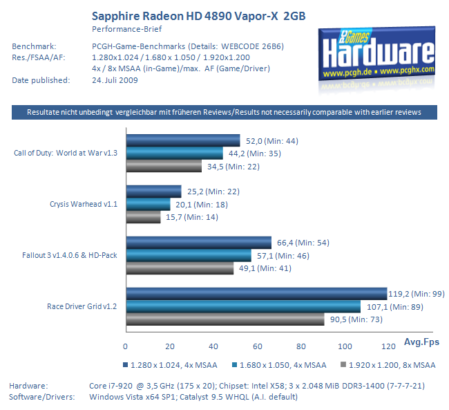
4890 2G vs 4890 1G:
PerformanceBrief-HD4890-VaporX2G-HD.png


PerformanceBrief-HD4890-VaporX2G-1.png


4890 1G ran out of mem at 19X12 8xAA in Crysis and modded Fallout 3.

5870 1G should be more vram limited.
 
Improving certain bits (that were flawed in the past) and increasing number of processing units, does not equate to a new architecture IMO and that's definitely not what's happening in Fermi. The changes go beyond just an increase of processing units and efficiency here and there.
The only noticeable things I can remember from RV670 vs RV770 were the improved ROPs and the memory controllers to support GDDR5.
Where the memory is concerned the entire memory architecture is different, moving from ring bus mechanism, to a localised memory subystem that also invloved changing the entire cache architecture as well; from a memory operation perepctive nothing is the same.

The SIMD structures are different, moving from texture units that serve across SIMD's to texture units that directly serve a SIMD. Each of the ALU's changed in strcuture, and also changed around functionality (for example, moving integer operations from one slot to all 5 slots). R6xx lacked a compute shader which was added to RV7xx that also came with LDS and GDS.

etc., etc.

Anyway, I think it's already established that the "new architecture" idea is a very subjective one, but there are certainly some concepts that are universal I believe. I guess that from your perspective, RV670 was also a new architecture, because it added DX10.1 support and to me "simple" additions do not make a new architecture
No, RV670 is very much part of the R6xx architecture, which was always designed to evloved as the DX0.1 spec did - R600 supported some DX10.1 capabilities, RV630 and RV610 more, and as the spec settled RV670, RV635 and RV620 all of them, but here was no architectural changes need to do that.

A complete (or almost complete) change in how the chip works internally, in terms of cache hierarchy, processing units configuration and inter-operability, certainly does and Fermi fits the bill. The last architecture from your side that fits that bill IMO, is R600.
And this definition certain fits for R6xx->RV7xx.
 
Because it's not scalar. Doh. There'd be a single ALU if it was scalar.

Jawed

Depends on how you define it I guess. If for each instruction the program is only exposed to a scalar unit then for all intents and purposes it's scalar. It doesn't matter if some other thread is running in parallel on the other scalar thingamagig next to it. The way I look at it, if there is no requirement for a single warp to occupy both the ALU and SFU units in a given cycle to achieve maximum occupation then it's scalar.

If you're talking about the fact that it's SIMD well is that really a useful argument when comparing GPU architectures. They're all SIMD so it's sorta irrelevant.
 
4- Predication.
G80 and GT200 had no predication?

7- More SPs per SM.
I think this is a big deal - the register file, operand collection and dependency scoreboarding all seem to have needed a re-work to account for the timing and bank count changes here.

12- Two warp schedulers.
Seems to be a variation on the old convoy based system.

13- Out of order thread block execution & completion.
G80 and GT200 have solely in-order block execution? If two blocks share a SM, the second cannot start until the first has completed? Can two blocks share an SM on those older GPUs? (Actually, thinking about it, I suspect not...)

Is this ordering constraint on the older GPUs solely intra-SM or is it across all SMs?

Jawed
 
I just wanna be sure... Have you noticed the "can be" in my post? "But this can be: http..."

You should be ashamed of not giving a proper answer, and hide in semantics, when you know what the intention was, how did it sound like.

Read 2 times before bashing.

What I said was that GF100 as a whole IS NOT revolutionary. Architecture, maybe. GF100 with all that problems in mind absolutely not.

You should read better too. What we are discussing when we say it is revolutionary is really the architecture, not the performance. So you are answering to who then? You are here just to bash Fermi and you are so blind about it (*cough* Charlie zealot *cough*), that you dont even read what people are discussing in reality.
 
Last edited by a moderator:
Depends on how you define it I guess. If for each instruction the program is only exposed to a scalar unit then for all intents and purposes it's scalar.
The compiler and the hardware don't see it like that. Hence all the grief with the "missing MUL". A problem "solved" in GF100 by deleting that MUL.

A perennial complaint from CUDA programmers is being unable to ascertain how the hardware issues the instructions and the nature of RAW dependencies and the effects on throughput. If the architecture exposed a scalar programming model these questions wouldn't exist (though some of these questions derive from memory latencies). There have been several attempts at characterising the hardware's execution model, in a bid to understand how to write efficient CUDA, or efficient PTX.

It's pretty strange NVidia makes the last mile so hard.

Jawed
 
4890 1G ran out of mem at 19X12 8xAA in Crysis and modded Fallout 3.
Cool, thanks, so we know Warhead is an invalid test then - 34% faster for the 2GB card is pretty amazing at only 1920.

CoD WaW and Grid see no benefit.

Fallout with HD pack: will watch out to see if that comes up on GF100 launch - seems unlikely.

Now what about the other games, like HAWX?

5870 1G should be more vram limited.
Why? Compared with what?

Jawed
 
Why? Compared with what?

Jawed

Wouldn't faster rendering speed mean you would be more frequently swapping out textures/whatever from memory in memory limited situations?

And if speed to swap out stuff in memory isn't proportionately speeded up then you'd spend a greater percentage of your time waiting.

Also, going to assume more games will be tested at 2560x1600 with 8xAA/16x AF with the release of Fermi. So there might be more situations of 1 GB framebuffer running into limitations in more games.

Since Eyefinity 6 with 2 GB should be released just prior to Fermi, that will be able show whether that's the case for 5870 or not.

Regards,
SB
 
Wouldn't faster rendering speed mean you would be more frequently swapping out textures/whatever from memory in memory limited situations?

And if speed to swap out stuff in memory isn't proportionately speeded up then you'd spend a greater percentage of your time waiting.
Agreed with all that. I'm curious what Mindfury meant: that or something more significant.

Also, going to assume more games will be tested at 2560x1600 with 8xAA/16x AF with the release of Fermi. So there might be more situations of 1 GB framebuffer running into limitations in more games.
It's going to be funny seeing some sites start testing 8xMSAA having routinely avoided it.

Since Eyefinity 6 with 2 GB should be released just prior to Fermi, that will be able show whether that's the case for 5870 or not.
Can AMD get its act together? Will AMD be sending out a Fermi Competitive Reviewer's Guide document on how to test ATI cards?

Jawed
 
Wouldn't faster rendering speed mean you would be more frequently swapping out textures/whatever from memory in memory limited situations?

And if speed to swap out stuff in memory isn't proportionately speeded up then you'd spend a greater percentage of your time waiting.
Yes, but that's only true IF you have to swap out things in the first place. So in the previous benchmarks, the two of them which showed absolutely no sign of being memory limited, still shouldn't be with a HD5870. However, the Fallout 3 one which only showed a mild performance decrease might have a much larger performance decrease with a HD5870 with 1GB ram. And Crysis Warhead (which already had a bit decrease) certainly too.
Those were 1920x1200 8xAA though. I think we might see a lot of 2560x1600 (with 4x/8xAA) in fermi reviews to further stress that point.
 
And the dark secret of GT200 is that it's the kludge that NVidia used, because G100 (now called GF100) was too ambitious for the end of 2007 :p
That's the first time I've heard this. Some evidence that it was planned much earlier?
Would be kinda like the mythical R400 I guess :).
 
Back
Top