
You are using an out of date browser. It may not display this or other websites correctly.
You should upgrade or use an alternative browser.
You should upgrade or use an alternative browser.
AMD: R9xx Speculation
- Thread starter Lukfi
- Start date
")
1920x1080 = 2073600 pixelsIs AMD's "right way" not to limited for devs?
They must use twice the size of triangles and stay between tessellation factor 4-12 to have a 50%+ increase over Cypress. And in this case they are only capable of 540 Mtris/s max - slighty more than a GTS450.
If each pixel = 1 triangle, we have 2 Mtris/frame.
For 40 FPS we needs 83 Mtris.
Add EyeFinity with 3 x 24" LCD: 3 x 83 Mtris = 249 Mtris.
Add 3D over EyeFinity: 2 x 249 Mtris = 498 Mtris.
If I made no mistake, EyeFinity 3D (1920x1080) with 1 triangle per pixel @ 40 FPS -> 498 Mtris.
Heaven 2.1 numbers from 6870: http://www.tomshardware.de/foren/241537-41-verkaufe-radeon-6870#t17807
Min-FPS is very low, no real improvement over a 5870. GTX460@715Mhz has 18,8 FPS, GTX480 35,4 FPS.
http://www.hexus.net/content/item.php?item=25391&page=6
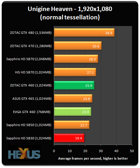
That appears to be the same settings as this german guys.

Man from Atlantis
Veteran
you are again wrong jimbo75
here a guy from anadtech forums did same settings with hairy overclocked GTX460 1gb@725MHz/3600MHz sli disabled
http://i482.photobucket.com/albums/rr185/notty222/Unigine_2010_10_20_17_23_54_726.png
here a guy from anadtech forums did same settings with hairy overclocked GTX460 1gb@725MHz/3600MHz sli disabled
http://i482.photobucket.com/albums/rr185/notty222/Unigine_2010_10_20_17_23_54_726.png
So maybe it tesselates maybe as same as 460. Good enough.
Thats at normal though.
Mintmaster
Veteran
People need to stop making these simplistic calculations. Triangles come in clumps. When you have a bunch of small or hidden triangles, there are very few pixels drawn to the screen during that time. You basically have to deal with those triangles and draw the majority of the scene in the remaining time.1920x1080 = 2073600 pixels
If each pixel = 1 triangle, we have 2 Mtris/frame.
For 40 FPS we needs 83 Mtris.
Add EyeFinity with 3 x 24" LCD: 3 x 83 Mtris = 249 Mtris.
Add 3D over EyeFinity: 2 x 249 Mtris = 498 Mtris.
If I made no mistake, EyeFinity 3D (1920x1080) with 1 triangle per pixel @ 40 FPS -> 498 Mtris.
Here's a more detailed post I did on the matter:
http://forum.beyond3d.com/showpost.php?p=1383571&postcount=481
What I don't understand is why ATI can't do one tessellated triangle per clock. Cypress was taking 3-6 clocks per triangle in tessellation tests, and it looks like this generation is barely any better.
What on earth is going on inside that tessellation engine? It's inexcusable to be drawing equivalent, bandwidth-wasting, pretessellated DX10 geometry faster than tessellated DX11 geometry.
EDIT: Maybe ATI was selling itself short with that slide if this benchmark is correct...
Last edited by a moderator:
Unknown Soldier
Veteran
Heaven 2.1 numbers from 6870: http://www.tomshardware.de/foren/241537-41-verkaufe-radeon-6870#t17807
Min-FPS is very low, no real improvement over a 5870. GTX460@715Mhz has 18,8 FPS, GTX480 35,4 FPS.
? Really?

Looks better to me. According to that pic, the 5870 did average of 25.8fps at 1920x1080.
Your pic
has an average of 34.3fps, I'd say quite an improvement.
Note that none of the cards actually are truly tesselation limited at these settings. Otherwise they wouldn't scale that well with resolution, and neither would the HD5870 be nearly twice as fast as the HD5770.has an average of 34.3fps, I'd say quite an improvement.
Makes that score hard to believe, I can't see what magic Barts would use to achieve that (but if it's real all the better...).
you are again wrong jimbo75
here a guy from anadtech forums did same settings with hairy overclocked GTX460 1gb@725MHz/3600MHz sli disabled
http://i482.photobucket.com/albums/rr185/notty222/Unigine_2010_10_20_17_23_54_726.png
That was with only 4x AF.
Give Nvidia a few percent due to recent drivers maybe, then that cpu at 4ghz and I think AMD might just have changed the tessellation game too.
If that german guys bench is legit, that is.
Jawed
Legend
I chose 4x4 right-angle triangles because it's been suggested that triangles of ~8 pixels area are small enough. This is merely an extreme bad case of ~8 pixel triangles, to show how an edge of roughly 4 pixels length can look nothing like a curve.You are mis-using tesselation and hardware capabilities the "circle" in the right could be rendered with just two triangles 4 pixels wide and 8 pixels high and letting them have at least 16 pixels area.
I presume you've seen:And just for reference, with 4 traingles one can significantly improve image quality by doing hexagons instead of squares, this just show how biased benchmarks are today by using supoptimal techniches just to decrease performance on one plataform.
http://www.humus.name/index.php?page=Comments&ID=228&start=16
Though games rarely render circles, they tend to render volumes with curved edges.
In the slide posted earlier:

the supposed 16-pixel triangle highlights something of a con in this pixels-per-triangle counting. It's actually a 24-pixel triangle, because it requires 6 quads in its rendering (without MSAA - obviously more with varying degrees of MSAA).
Similarly the square I posted is really composed of 12-pixel triangles.
Which opens up the question of what they really mean. I think they really mean 4-quad triangles, not 16 pixel triangles.
Also, counting quads rather than pixels actually helps ATI, because the triangles will tend to have less area when counting pixels.
Man from Atlantis
Veteran
5870 with cf disabled
http://i283.photobucket.com/albums/kk293/luv2eather/Computer/Uni5870.jpg
same as 6870
http://i283.photobucket.com/albums/kk293/luv2eather/Computer/Uni5870.jpg
same as 6870
That was with only 4x AF.
Nope, they used 4xAF and 4xMSAA
You can see the setting screen, too.Heaven v2.1 was set to high shaders, with 4x AF, and 4x AA, on normal tessellation mode with DirectX 11.
? Really?
Looks better to me. According to that pic, the 5870 did average of 25.8fps at 1920x1080.
They write nothing about the settings.
5870 with cf disabled
http://i283.photobucket.com/albums/kk293/luv2eather/Computer/Uni5870.jpg
same as 6870
Overclock on your gpu?
Jawed
Legend
http://v3.espacenet.com/publication...T=D&date=20091203&CC=US&NR=2009295804A1&KC=A1What on earth is going on inside that tessellation engine? It's inexcusable to be drawing equivalent, bandwidth-wasting, pretessellated DX10 geometry faster than tessellated DX11 geometry.
Has a hint about off-die buffer usage for GS:
[0008] Rendering costs during geometry shading are attributed to the ALU instructions required to process each primitive, the computing bandwidth associated with vertex lookup from the vertex shader's memory, and the computing bandwidth required to load the processed data into memory. Oftentimes, similar to the vertex shader, data processed by the geometry shader data is loaded into a memory device.
[0009] Rendering costs attributed to the vertex and geometry shaders can dominate the total rendering cost of the graphics pipeline. For some applications, the rendering costs attributed to the vertex and geometry shader may be unavoidable due to design constraints such as performance and circuit area of the GPU. For instance, for a high volume of primitive data entering the graphics pipeline, the geometry shader may emit a large number of primitives for each vertex processed by the vertex shader. Here, off-chip memory may be required such that latency periods between the vertex shader and geometry shader operations can be hidden. In the alternative, potential latency issues can be resolved by adding on-chip memory to the GPU, thus increasing overall circuit area. However, an increase in circuit area of the GPU is counterbalanced by manufacturing costs associated with the fabrication of a larger graphics chip. Thus, in light of performance and cost factors, off-chip memory may be a feasible solution for many GPU designs.
[0010] In situations where a low volume of primitive data enters the graphics pipeline and the geometry shader does not emit a large number of primitives for each vertex processed by the vertex shader, then the loading of processed data into, and retrieving of the data from, off-chip memory can be inefficient. Here, a latency period between the vertex shader and geometry shader operations can increase (relative to processing time) due to a small number of primitives being emitted from the geometry shader. In other words, since the geometry shader emits a small number of primitives, the computing time associated with retrieving data from the vertex shader's memory and loading data processed by the geometry shader into off-chip memory is more than the computing time for the geometry shader to emit primitives. As the geometry shader processes more vertex data with a small number of emits, the latency period of the geometry shader's operation increases, thus increasing the overall rendering cost of the graphics pipeline.
Perhaps this GS buffering is always active when tessellation is active? Would Evergreen be dumping vertices into memory post-GS, only to retrieve them for setup, whenever TS is active?
But would that "fixed latency" actually matter in tessellation scenarios?
Perhaps that fixed latency would only be seen in lower-factor tessellation (i.e. where triangle sizes fluctuate widely, so the bottleneck dances between TS and RS)? So the impact of storing vertex data on-die (the subject of the patent application) would only be seen with the lower factors, something seen in that graph of HD6870's gain over HD5870?
Man from Atlantis
Veteran
Overclock on your gpu?
its not mine and dont think its overclocked.. oh cmon..
Nope, they used 4xAF and 4xMSAA.
Sorry I mean "only" 4xAF compared to 16x.
its not mine and dont think its overclocked.. oh cmon..
Oh come on what?
There are a bunch of reviews on the web showing the gtx 460 scoring between 25 and 30 fps at normal settings, with highly overclocked cpu's.
I'm more inclined to trust those compared to some random blokes on Anandtech.
Man from Atlantis
Veteran

One more thing, is MLAA and improved AF something that will be found in CCC for both 5000 and 6000 series or is that hardware specific for the 6000 series?
The improved AF might be hardware specific to the 6xxx series, but the MLAA is post-process, not done by a specific function in the hardware. If it doesn't come to the 5xxx and earlier series', it's due to AMD policies, not hardware limitation.
Similar threads
- Replies
- 3K
- Views
- 645K
- Replies
- 1K
- Views
- 374K
- Replies
- 12K
- Views
- 2M
- Replies
- 6
- Views
- 5K